Contents
- Highlights
- 100G Ethernet PCB: Definition and Scope
- 100G Ethernet PCB Rules and Specifications
- 100G Ethernet PCB Implementation Steps
- 100G Ethernet PCB Troubleshooting
- Supplier Qualification Checklist: How to Vet Your Fab
- Glossary
- 6 Essential Rules for 100G Ethernet PCB (Cheat Sheet)
- FAQ
- Request a Quote / DFM Review for 100G Ethernet PCB
- Conclusion
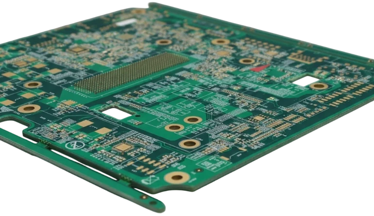
In the world of high-speed networking, a 100G Ethernet PCB is not just a standard circuit board with tighter tolerances; it is a precision-engineered component where every micron of copper and every weave of glass fiber impacts signal integrity. Specifically, these boards are designed to support data transmission rates of 100 Gigabits per second (Gbps), typically achieved through four lanes of 25 Gbps (NRZ) or two lanes of 50 Gbps (PAM4). At these frequencies, the PCB trace acts less like a simple wire and more like a transmission line, where dielectric loss, skin effect, and via stubs can completely destroy the signal eye diagram before it reaches the receiver.
As a Senior CAM Engineer at APTPCB, I review hundreds of high-speed designs annually. The difference between a working 100G prototype and a failed board often comes down to material selection (moving away from standard FR4) and the physical management of signal transitions (vias). This guide covers the critical manufacturing and design rules necessary to achieve first-pass success.
Quick Answer
For a functional 100G Ethernet PCB, you must control insertion loss and return loss strictly across the Nyquist frequency (typically 12.89 GHz for 25G NRZ).
- Material Rule: Do not use standard FR4 (Tg170). You must use "Low Loss" or "Ultra Low Loss" laminates (e.g., Panasonic Megtron 6/7, Isola Tachyan, or Rogers RO4000 series) with a Dissipation Factor (Df) < 0.005.
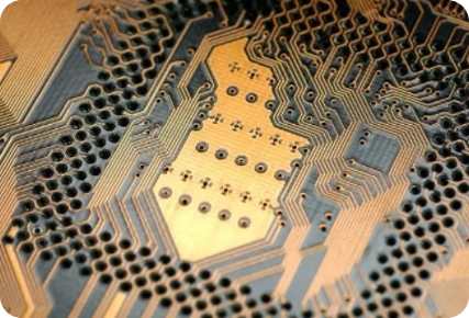
- Critical Pitfall: Via Stubs. Any unused portion of a plated through-hole via acts as an antenna, causing resonance that kills signals. You must use backdrilling or blind/buried vias to reduce stubs to < 10 mils (0.25mm).
- Verification: Impedance is not enough. You need Insertion Loss testing using a VNA (Vector Network Analyzer) to verify the transmission line quality, not just the characteristic impedance.
- Copper Profile: Specify VLP (Very Low Profile) or HVLP (Hyper Very Low Profile) copper foil to minimize skin effect losses.
- Stackup: Always use a symmetrical stackup with tightly coupled differential pairs referenced to solid ground planes.
Highlights
- Material Matters: Switching from standard FR4 to Megtron 6 can improve insertion loss by over 50% at 12 GHz.
- Backdrilling is Mandatory: For through-hole connectors on thick backplanes, backdrilling is the most cost-effective way to remove signal-killing stubs.
- Fiber Weave Effect: At 25Gbps+ per lane, the glass weave pattern matters. Use "spread glass" (e.g., 1067, 1078) or route traces at a slight angle (10°) to avoid skew.
- Surface Finish: ENIG or Immersion Silver are preferred for their flat surface; avoid HASL due to unevenness affecting impedance.
- Tolerances: 100G designs require impedance control of ±5% or better, tighter than the standard ±10%.

100G Ethernet PCB: Definition and Scope
A 100G Ethernet PCB is defined by its ability to support the IEEE 802.3bj (100GBASE-KR4) or 802.3bm standards. While "100G" refers to the aggregate throughput, the engineering challenge lies in the per-lane speed. Most 100G implementations use 4 lanes of 25 Gbps (NRZ signaling). Newer implementations might use 2 lanes of 50 Gbps (PAM4 signaling).
The physics of 25+ Gbps signals means that the board material itself absorbs signal energy (dielectric loss), and the roughness of the copper traces increases resistance at high frequencies (skin effect). Furthermore, the margin for error in timing (skew) drops to picoseconds. If the positive and negative legs of a differential pair are not perfectly matched in length—or if one leg travels over a glass bundle while the other travels over resin—the signal arrives out of phase, closing the "eye" and causing data errors.
At APTPCB, we categorize 100G boards as "Ultra High-Speed," requiring specific lamination cycles and drilling protocols to ensure the physical board matches the simulation data.
Tech / Decision Lever → Practical Impact
| Decision Lever / Spec | Practical Impact (Yield/Cost/Reliability) |
|---|---|
| Laminate Df (Dissipation Factor) | Directly dictates maximum trace length. Lower Df (<0.004) allows longer traces but increases material cost by 2-3x vs FR4. |
| Copper Foil Roughness (VLP/HVLP) | Smoother copper reduces insertion loss at high frequencies (Skin Effect). Essential for runs > 10 inches at 25GHz. |
| Backdrilling (Stub Removal) | Removes resonant stubs. Mandatory for signal integrity but adds a drilling process step and requires specific design clearances. |
| Glass Weave Style (1067/1078) | Using "spread glass" minimizes the "Fiber Weave Effect" (skew), preventing periodic jitter without needing complex zig-zag routing. |
100G Ethernet PCB Rules and Specifications
Designing for 100G requires adhering to strict rules that govern the geometry of the traces and the materials used. Below is a breakdown of the standard specifications we recommend for manufacturing at APTPCB.
| Rule / Parameter | Recommended Value | Why it matters | How to verify |
|---|---|---|---|
| Differential Impedance | 85Ω or 100Ω ±5% | Mismatches cause reflections (Return Loss), reducing signal power at the receiver. | TDR (Time Domain Reflectometry) on coupons. |
| Trace Width/Space | 4mil / 5mil (min) | Tighter coupling reduces crosstalk; width affects skin effect loss. | AOI (Automated Optical Inspection) & Cross-section. |
| Via Stub Length | < 10 mils (0.25mm) | Long stubs act as notch filters, killing specific frequencies. | X-Ray inspection & Backdrill depth control logs. |
| Intra-Pair Skew | < 5 mils (approx 0.7ps) | Phase mismatch closes the signal eye diagram (differential to common mode conversion). | Design software check & VNA measurement. |
| Material Dk / Df | Dk ~3.0-3.6 / Df < 0.004 | Low Dk reduces propagation delay; Low Df reduces signal attenuation. | Material datasheet certification (IPC-4101). |
| Reference Plane | Solid Copper (GND) | Splits in the reference plane create massive inductance loops and EMI. | Visual inspection of Gerber files. |
For complex stackups, utilizing our PCB Stack-up services early in the design phase can help validate that your impedance targets are achievable with standard dielectric thicknesses.
100G Ethernet PCB Implementation Steps
Implementing a 100G design is a linear process where skipping a step usually results in a board spin.
Implementation Process
Step-by-step execution guide
Select a low-loss laminate (e.g., Megtron 6). Define layer counts to ensure every high-speed signal layer has an adjacent solid ground reference. Calculate trace widths for 100Ω impedance.
Route 100G differential pairs first. Minimize vias. Use "teardrops" on pads. Ensure BGA breakout regions maintain impedance and ground referencing. Avoid 90° bends; use 45° or arcs.
Run post-layout simulations. Check for crosstalk (NEXT/FEXT) and return loss. Identify via stubs that exceed 10 mils and mark them for backdrilling in the fabrication notes.
Send Gerber files with specific drill charts for backdrilling. Request TDR reports and, if possible, SET2DIL or SPP testing to verify insertion loss on test coupons.
100G Ethernet PCB Troubleshooting
Even with good design, issues can arise during testing. Here are common failure modes for 100G links and how to address them.
1. High Bit Error Rate (Ber)
If the link establishes but drops packets, the issue is often Jitter or Crosstalk.
- Cause: Traces routed too close to aggressive aggressor signals (like DC-DC converters or other high-speed clocks).
- Fix: Increase spacing between differential pairs (3W rule is often insufficient; aim for 4W or 5W). Check for gaps in the reference plane (return path discontinuity).
2. Signal Attenuation (Insertion Loss Failure)
The signal is too weak at the receiver.
- Cause: Trace length is too long for the chosen material, or the copper is too rough.
- Fix: If you cannot shorten the trace, upgrade to a lower Df material (e.g., move from Megtron 4 to Megtron 7). Specify HVLP copper foil.
3. Resonance / Notch Filtering
The signal looks good at low frequencies but vanishes at a specific high frequency (e.g., 12 GHz).
- Cause: Via Stubs. The unused portion of the via is resonating at a quarter-wavelength of the signal frequency.
- Fix: Implement Backdrilling to remove the stub. Ensure the backdrill depth tolerance is tight (typically ±0.05mm).
Supplier Qualification Checklist: How to Vet Your Fab
Not every PCB manufacturer can handle 100G requirements. Use this checklist to vet your supplier (like APTPCB) before placing an order.
- Does the fab have in-house VNA testing capabilities? (Essential for verifying insertion loss, not just impedance).
- What is the standard backdrill depth tolerance? (Should be ±0.1mm or better; ideally ±0.05mm).
- Do they stock High-Speed Laminates? (Ask specifically for Megtron 6/7, Rogers 4350, or equivalent. If they have to order it, lead time increases).
- Can they handle +2/-2 mil trace width tolerance? (Standard is ±20%; high speed often needs ±10% or ±0.5mil).
- Do they perform cross-section analysis on every batch? (To verify plating thickness and dielectric layer consistency).
- Is X-Ray inspection used for backdrill verification? (To ensure the drill didn't cut too deep or leave too much stub).
Glossary
- Insertion Loss: The loss of signal power as it travels down the trace, measured in decibels (dB). Higher frequencies suffer more loss.
- Return Loss: The amount of signal reflected back to the source due to impedance mismatches. High return loss means poor signal integrity.
- Backdrilling: A manufacturing process where a drill bit slightly larger than the via hole is used to drill out the unused barrel (stub) of a plated through-hole, reducing signal reflection.
- PAM4 (Pulse Amplitude Modulation 4-level): A modulation scheme that transmits two bits per symbol, effectively doubling the data rate compared to NRZ (Non-Return-to-Zero) at the same bandwidth, but requiring better Signal-to-Noise ratio.
- Skew: The time difference between the arrival of the positive and negative signals in a differential pair. High skew converts differential signals to common-mode noise.
6 Essential Rules for 100G Ethernet PCB (Cheat Sheet)
| Rule / Guideline | Why It Matters (Physics/Cost) | Target Value / Action |
|---|---|---|
| Remove Via Stubs | Stubs act as antennas, causing severe resonance and signal loss at 25GHz+. | Backdrill to < 10 mils remaining. |
| Use Low-Loss Material | Standard FR4 absorbs too much signal energy at high frequencies. | Df < 0.005 (e.g., Megtron 6). |
| Continuous Reference Plane | Return path current must flow directly under the signal. Gaps cause inductance spikes. | Solid Copper (No splits under traces). |
| Ground Vias Near Signal Vias | Provides a return path for the current when the signal changes layers (Z-axis). | Place GND via within 30 mils of signal via. |
| Tight Impedance Control | Mismatches cause reflections. 100G is less forgiving than 10G. | ±5% Tolerance (vs standard ±10%). |
| Mitigate Fiber Weave | Periodic glass bundles cause skew if one trace runs on glass and the other on resin. | Use Spread Glass or Zig-Zag routing. |
FAQ
Q: Can I use standard FR4 for 100G Ethernet PCBs?
A: Generally, no. While it might work for extremely short traces (< 1 inch), standard FR4 has a Dissipation Factor (Df) that is too high (approx 0.02), leading to excessive signal loss at 12-14 GHz. You should use mid-loss or low-loss materials like Isola FR408HR or Panasonic Megtron 6.
Q: What is the cost difference between standard FR4 and High-Speed materials?
A: High-speed laminates like Megtron 6 can cost 2x to 3x more than standard FR4. However, the material cost is often a fraction of the total board value, and the cost of a failed prototype due to signal integrity issues is much higher.
Q: Do I need blind and buried vias for 100G?
A: Not necessarily. While blind/buried vias are excellent for reducing stubs, they increase lamination cycles and cost. Backdrilling is a cheaper alternative for through-hole vias that achieves similar signal integrity results for 100G applications.
Q: How do I calculate the correct impedance for 100G?
A: You can use an Impedance Calculator, but for 100G, we recommend consulting with your fabricator. We use field-solver software (like Polar SI9000) that accounts for resin content, copper roughness, and etchback to give you the exact trace width needed.
Q: What surface finish is best for 100G PCBs?
A: ENIG (Electroless Nickel Immersion Gold) or Immersion Silver are recommended. They provide a very flat surface for component mounting and do not add irregular thickness to the traces like HASL (Hot Air Solder Leveling), which can disrupt impedance.
Q: What is the maximum trace length for 100G on a PCB?
A: This depends on the material. On standard FR4, you might get 2-3 inches. On Megtron 6, you can often achieve 10-15 inches or more, depending on the retimer/driver capabilities. Simulation is required to determine the exact reach.
Request a Quote / DFM Review for 100G Ethernet PCB
Ready to move your high-speed design to production? At APTPCB, we specialize in Advanced PCB Manufacturing for data center and networking applications.
To get an accurate quote and DFM, please send:
- Gerber Files (RS-274X format preferred).
- Fabrication Drawing specifying drill chart and backdrill layers.
- Stackup Details (Layer count, desired material, and impedance requirements).
- Netlist (IPC-356) for electrical testing verification.
Conclusion
Designing a 100G Ethernet PCB requires a shift in mindset from "connecting points" to "managing transmission lines." By selecting the right low-loss materials, strictly controlling via stubs through backdrilling, and adhering to tight impedance tolerances, you can ensure your board performs reliably at 25 Gbps per lane and beyond.
Don't let signal integrity be an afterthought. Engage with your manufacturer early to validate your stackup and design rules.
Signed, The Engineering Team at APTPCB