PCB + PCBA · First article

First article.Evidence for release.

Connect the first build to approved drawings, measured characteristics and the customer’s production release.
FAI scope
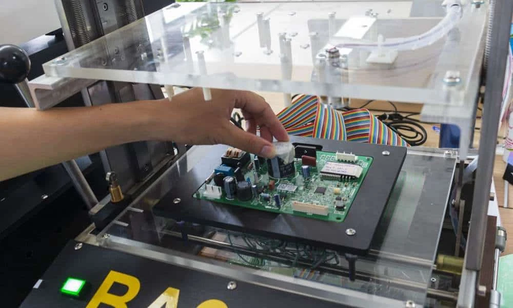
An operator connecting a populated circuit board on an electrical test fixture
Electrical verification is included when it forms part of the agreed FAI scope.

01 / First-build baseline

Establish what the first article must prove.

APTPCB is a PCB manufacturing and PCB assembly (PCBA) provider focused on stable quality and reliable mass production. As part of our standard quality workflow, we perform First Article Inspection (FAI) on new and changed projects to make sure the boards we build for you match your design before we move into full volume.
FAI is not a standalone service we sell separately. It is an integrated step in our PCB & PCBA production process to help you reduce risk on new designs and revisions, shorten approval time with your own customers, and build a stable, repeatable production baseline.
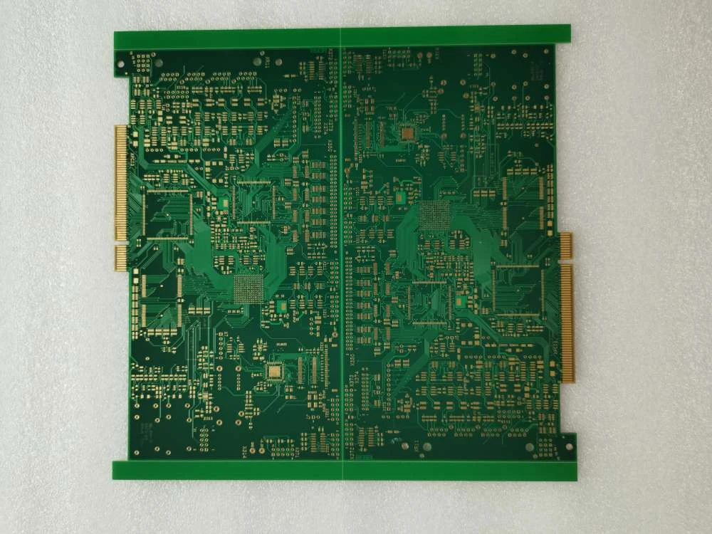
Unpopulated green circuit board with fine copper features and component lands
Bare-board dimensions, features and connectivity require their own acceptance basis.

02 / The FAIR package

Put the revision, measurements and records in one package.

You don't just receive a 'good sample'; you get documentation you can use internally or with your own customers. If you need a specific format (e.g. AS9102-style forms or a customer template), we can prepare the FAI package according to that structure as long as it's clearly defined at order stage. A typical FAI / FAIR package from APTPCB may include:

FAIR evidenceRequired record
01Part number and revision identification
02Reference to drawings, specs, and BOM used
03List of measured characteristics (dimensions, thickness, key features) with results
04Material and process details (laminate, copper weight, surface finish, solder process, etc.)
05Photos of the board / assembly and key areas
06Electrical or functional test results (when part of FAI scope)

Scroll the table to review all columns.

03 / Fabrication & assembly
Inspect the board and the assembly against their own requirements.

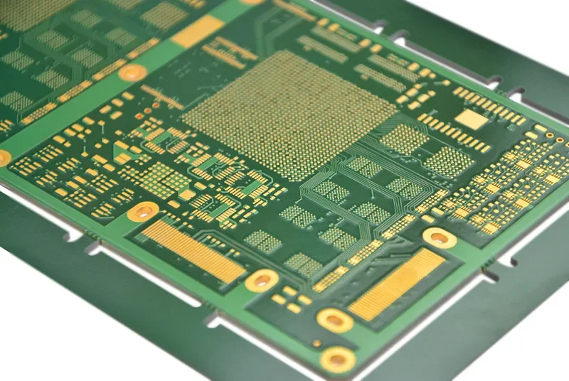
Close-up of a bare circuit board with fine-pitch pads and gold contacts
Bare-board features and dimensions can be checked against the approved fabrication data.

What We Check During FAI for PCB Manufacturing

For bare PCB manufacturing, our FAI typically covers:

Board Dimensions & Features:

  • Overall board size and outline
  • Hole sizes, positions, and tolerances
  • Slot dimensions and mechanical cut-outs
  • Board thickness (overall and, if required, core / prepreg)

Copper & Layer Structure:

  • Trace width and spacing on each critical layer
  • Annular ring and land sizes for plated holes
  • Layer registration and alignment (inner and outer layers)
  • Surface finish type and thickness (ENIG, HASL, immersion silver, etc.)

Materials & Stack-Up:

  • Laminate type and Tg as specified
  • Copper weight per layer (e.g. 1 oz, 2 oz, etc.)
  • Solder mask color, coverage and alignment
  • Silkscreen clarity and placement

Electrical & Special Requirements (When Applicable):

  • Electrical test: continuity and isolation
  • Controlled impedance test results (for high-speed designs)
  • Any special tests agreed in advance (peel strength, warpage, etc.)
All findings are documented and linked to your part number and revision, forming the baseline for ongoing PCB production.

What We Check During FAI for PCBA (Assembly)

If you also place PCBA assembly with APTPCB, the First Article Inspection at assembly level focuses on:

Component & BOM Compliance:

  • Correct components loaded versus your BOM
  • Part number, value, and package verification for key components
  • Substitution control as per your approval (if any)

Placement & Orientation:

  • Placement accuracy on fine-pitch ICs, BGAs, connectors, etc.
  • Polarity and orientation of polarized parts (diodes, electrolytic capacitors, ICs, LEDs, etc.)
  • Alignment of connectors, switches and mechanical interfacing parts

Solder Quality (with AOI & Visual):

  • Solder joint shape and coverage on SMT and THT parts
  • Bridges, tombstones, insufficient or excess solder
  • Rework areas, if any, checked against standards

Basic Electrical / Functional Checks (If in Scope):

  • Power-on and basic current consumption check
  • Simple functional checks (e.g. LEDs, buttons, communication ping)
  • Or a defined Functional Test if you provide or request a test spec
After FAI approval, the same assembly programs, stencil, reflow profile and test flow are used for mass production, ensuring consistency across all shipments.

04 / Change control

Recognize the changes that reopen first-article review.

We apply First Article Inspection in situations where quality risk is naturally higher, for example:

New PCB or PCBA design (NPI)

Confirm the inspection requirement at order release.

Major design revision

(layout changes, stack-up changes, new components)

Change of material or key process

(laminate, surface finish, soldering process, etc.)

New tooling or new production line

for your project

Customer-specified FAI / FAIR requirement

(e.g. aerospace, automotive, industrial projects)

05 / Trial → Approval → Production

Make the release decision before the volume build.

The first article belongs to a controlled build route, with customer review between the trial lot and volume production.
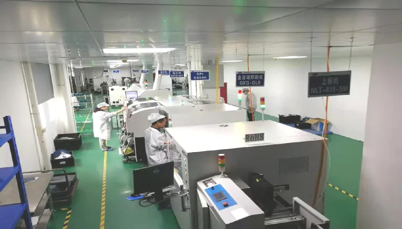
Surface-mount assembly and inspection equipment on a production line
Whenever you start a new project or major change with APTPCB, your order goes through a structured flow:
01

DFM / DFA review

– we check manufacturability and assembly feasibility.
02

Tooling & process setup

– stack-up, materials, programs, stencils, fixtures.
03

Trial build / first lot

– we fabricate and (if needed) assemble your first batch.
04

First Article Inspection (FAI)

– we verify the first piece against your requirements.
05

Customer approval

– you review the FAI results and samples.
06

Stable mass production

– only after FAI is passed and confirmed.

06 / Engineering handoff

Specify the approval package with the order.

You don't need to manage FAI as a separate 'service'. Simply:
Send your RFQ with Gerber / CAD data, BOM (for PCBA), drawings and key specs
Tell us your FAI expectations – PCB only, or PCB + PCBA; required documents / format (if any); any special characteristics to highlight
We will include FAI planning into our quotation and production plan for new or changed projects.
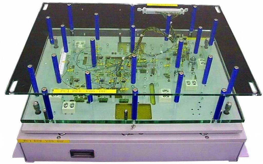
Test fixture with a circuit board, locating posts and an upper support plate
Fixture access and board support are part of the electrical test review.

Partner with APTPCB for PCB & PCBA with Built-In First Article Inspection

If you are preparing to launch a new board or move an existing one to a new supplier, and you want reliable PCB manufacturing, PCB assembly, and built-in First Article Inspection, APTPCB is ready to support you from prototype through mass production.

Our integrated FAI process ensures that your first production run is not a gamble—it's a validated, documented step toward stable, repeatable quality. Contact us today to discuss your PCB and PCBA needs.

ENGINEERING REFERENCE

Additional FAI coverage and customer benefits

What This Means for You as a Customer
By choosing a PCB manufacturer and PCB assembly partner that embeds FAI into the process, you get practical advantages:

Lower Risk on New Projects:

Issues are found and fixed on the first build, not after several lots
Design or documentation gaps are surfaced early

Easier Internal & Customer Approval:

Clear, structured FAI documentation you can attach to your own quality records
Faster sign-off with engineering, quality and key accounts

More Stable Mass Production:

Once FAI is approved, production runs follow the same validated process
Changes that require a new FAI can be clearly tracked and discussed

Stronger Message to Your Own Market:

You can confidently tell your customers that your boards are manufactured and assembled by a professional PCB manufacturing & PCB assembly company, with First Article Inspection built in for new designs and changes.
This directly supports your own quality positioning and brand trust.
FAI Scope & Coverage

PCB Only

Board dimensions, copper structure, materials, stack-up, electrical tests, and surface finish verification.

PCBA Assembly

Component compliance, placement accuracy, solder quality, and basic functional checks.

Documentation

Comprehensive FAIR report with measurements, photos, test results, and material details.

Custom Formats

AS9102 forms, customer templates, or specific documentation requirements as needed.

Risk Reduction

Early detection of design or process issues before mass production ramp.

Production Baseline

Validated process becomes the standard for all subsequent production runs.

PRACTICAL QUESTIONS

Scope, acceptance and practical limits

When is First Article Inspection required for a PCBA order?
FAI is required when starting a new project, a major design revision, a material or process change, new tooling, or when a customer specifies it in the order. For repeat orders with stable history, regular process control and final inspection are used instead of a full FAI every cycle. APTPCB may also propose FAI proactively when risk indicators are present.
What is the difference between FAI and electrical test for PCBA?
FAI checks that the first-assembled board matches the design intent — correct components, values, placement, orientation, and solder quality. Electrical test (ICT, flying probe, or functional test) checks that the circuit works correctly. FAI is a conformance gate; electrical test is a functional verification. Both are separate quality steps that can overlap in scope but serve different purposes.
What documentation does APTPCB provide after FAI approval?
The FAI package includes part-number and revision identification, reference to drawings and BOM used, a list of measured characteristics with results, material and process details, photos of the board and key areas, and electrical or functional test results when they are within FAI scope. For aerospace or automotive programs, AS9102-style forms or a customer-specified template can be prepared if defined at order stage.
Can FAI be performed without a complete BOM?
No. A complete and approved BOM is a prerequisite for FAI because the inspection verifies that every component loaded matches the specified part number, value, and package. Without a BOM, there is no reference standard against which to measure conformance. BOM preparation and cleanup should be completed before tooling and first-article setup begins.
How long does PCBA FAI typically take?
FAI timeline depends on board complexity, component count, and inspection scope. A simple 2-layer board with 50 components may take 1–2 working days; a complex 10-layer high-density assembly with 500+ components and ICT/FCT coverage may take 3–5 working days. The timeline is agreed during RFQ review and confirmed before tooling setup.

ENGINEERING & PRODUCTION REVIEW

Define your first-article approval.

Share the released design and the evidence your team needs before volume production.

  • Gerber / CAD and drawing revision
  • Approved BOM for assembly
  • Critical characteristics and tolerances
  • FAIR template and approval requirements