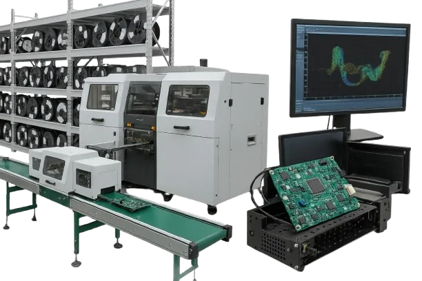
Rigid PCB Capability
18-layer FR4 builds with blind/buried vias, ±5% impedance releases, and Class 3 documentation tuned for server, medical, and industrial platforms.
Manufacturing Capabilities
60–80 µm build-up dielectric control, 0.075–0.10 mm laser microvias, ±5% TDR releases, 25 µm AOI / 5 µm AXI, and ionic cleanliness down to ≤0.78 µg/cm² keep compute, RF, medical, and aerospace builds audit-ready.
Mirror RayMing's catalog structure with rigid, flex, HDI, metal-core, SMT, and lab programs so sourcing teams can land on the right path instantly.
18-layer FR4 builds with blind/buried vias, ±5% impedance releases, and Class 3 documentation tuned for server, medical, and industrial platforms.
Dynamic flex and LCP stackups with adhesiveless copper, coverlay registration ≤35 µm, and bend qualification for wearables and radar harnesses.
3–12 layer flex cores laminated to rigid sections with laser depth checks, epoxy-filled transitions, and press-fit fixturing for aerospace harnesses.
1+N+1 to 5+N+5 HDI with 0.10 mm microvias, copper-filled VIPPO, and sequential lam presses logging delta-T/pressure every 30 seconds.
Metal-core and heavy copper platforms with >12 W/m·K thermal paths, copper coins, and flatness controls above 150 °C continuous use.
01005 and 0.20 mm pitch placement, inline SPI/AOI/AXI, ICT/boundary scan, and serialized travelers from prototype through mass production.
Orbotech LDI, YAG/CO₂ lasers, vacuum lamination, and SPC-driven plating centers visualized inside the facilities tour.
Panasonic/ASM SMT lines with selective solder, conformal coat, and robotic depanel plus automated stencil cleaning routines.
Reference designs, evaluation boards, and turnkey box-build examples ready for procurement teams to benchmark.
Cross-section, TDR, ion chromatography, and failure analysis labs with <15 minute logging between checkpoints.
ISO/IATF/AS9100 credentials, PPAP templates, and audit-ready control plans maintained by the compliance team.
Environmental stress, HALT/HASS, and burn-in chambers plus electrical validation bays for system-level sign-off.
Choose a process area to drill into detailed capability notes.
0.075–0.10 mm laser microvias with 60–80 µm dielectric spacing and copper-filled VIPPO keep planarity ≤15 µm while ΔR stays ≤10% through 1,000 IST cycles.
Up to four sequential presses log temperature/pressure every 30 s, hold registration within ±25 µm, and keep dielectric growth within ±5% for controlled-impedance coupons.
1+N+1 to 5+N+5 builds use ≤100 µm microvias and resin-filled VIPPO to route 0.35 mm BGAs; stacked vias are X-rayed after each lamination cycle.
Mechanical drilling supports 0.25 mm holes through 2.4 mm cores (10:1 AR) and pulse plating delivers ≥25 µm barrel copper verified by microsections.
Depth-controlled backdrill leaves ≤0.15 mm residue with ±75 µm depth accuracy while TDR overlays prove 92–100 Ω differential targets.
Expanded holes hold ±0.025–0.05 mm, barrel copper remains 25–28 µm after ream, and ionic cleanliness stays ≤1.56 µg/cm² to protect insertion force.
Copper-filled via-in-pad structures keep planarity ≤15 µm, void area <5%, and laser diameters at 0.075–0.10 mm for 0.35 mm pitch packages.
Coupons sweep 100–4000 MHz with solder-mask offsets (−2 Ω SE / −8 Ω diff) recorded so stackups release within ±5% tolerance.
Inline AOI captures 25 µm detail while 130 kV 3D X-ray resolves 5 µm voxels; BGA voids stay ≤20% and copper fill evidence is archived per lot.
Flying probe touches 0.10 mm pads, hipot pushes 500 V, and Kelvin continuity stay ≤20 mΩ with IPC-9252 reporting on every lot.
Embedded/buried/I-coins add >12 W/m·K thermal paths, hold planarity above 150 °C continuous use, and pass ±125 °C cycling for 500 cycles.
Electroless nickel 3–6 µm plus 0.05–0.125 µm gold keeps CSP pads flat and vacuum-packed panels retain >12 months of solderability.
3–5 µm nickel, 0.10–0.15 µm palladium, and 0.05 µm gold provide wire-bond readiness with phosphorus <9% to mitigate black-pad risk.
Edge fingers receive 1–1.5 µm hard gold over 3–6 µm nickel with chamfer ±3° and wear testing beyond 500 mating cycles.
Lead-free HASL controls solder thickness at 1–40 µm with ≤25 µm planar swing while cleanliness remains ≤1.56 µg/cm².
0.20–0.50 µm OSP films survive double reflow within 12 h and neutral rinses hold copper color shift to ΔE <2.
0.12–0.25 µm silver layers keep contact resistance <10 mΩ and sulfur barriers maintain whiteness for 12 months of storage.
0.8–1.2 µm tin with a 150 °C/1 h post-bake suppresses whiskers and limits intermetallic growth to <1.5 µm.
LDI-written masks enforce ≥0.10 mm dams, color-specific bridges of 5.5–7.5 mil, and single-side via plugs capped at 35.4 mil drills.
ROSE testing holds Class 2 at ≤1.56 µg/cm² and Class 3 at ≤0.78 µg/cm², with SIR coupons ≥100 MΩ after 85 °C/85% RH.
From prototype through NPI to mass production, choose the lane that fits your phase.
12–72 h expedite lots cover 2–8 layers with ±5% impedance coupons and full ionic reports before shipment. Travelers capture lamination data every 30 s for EVT sign-off.
10–1,000 piece lots run on dedicated HDI presses where drill/copper Cpk stays ≥1.33. Engineering change requests close inside 24 h so EVT → DVT moves without delay.
High-volume lines exceed 30k pcs/month with SPC on hole diameter, plating thickness, and solder mask alignment. MES serialization keeps PPAP and AS9100 genealogy one scan away.
Prototype SMT handles 0.20 mm pitch/01005 parts with 3D SPI height ±3% and 130 kV X-ray coverage ≥98%. Line changeovers stay under 30 min for multi-product days.
Inline SMT delivers 80k CPH with AOI escape <50 ppm, ICT coverage ≥95%, and boundary-scan nodes signed off before ramp. Serialization ties torque, coating, and burn-in data to each PCB.
Explore core process areas with curated resources.
Every build follows a documented playbook that keeps stackup, fabrication, and validation aligned.
Laminate libraries span Dk 3.2–10.2 with thickness targets ±10 µm so solver predictions and coupon models release within ±5% of impedance targets.
Rule decks flag annular ring <100 µm, solder mask relief <0.10 mm, and via AR >10:1. Annotated Gerber, IPC-2581, and ODB++ packages return in <24 h with risk-ranked findings.
Sequential lamination logs temperature/pressure every 30 s, copper plating is sampled to keep barrels ≥25 µm, and laser drilling records ±25 µm alignment on every HDI layer.
TDR (100–4000 MHz), AOI 25 µm, 5 µm AXI, and ROSE ≤1.56 µg/cm² are embedded in the traveler. Deviations auto-trigger 8D actions and re-measurements before release.
Structured controls and documentation keep projects compliant and auditable.
In-house equipment keeps inspection, test, and cleanliness loops tight.
130 kV 3D AXI resolves 5 µm voxels to validate copper fill, VIPPO voids (<5%), and BGA voiding (≤20% area) with SPC on depth maps.
Flying probe exercises 100% nets at up to 500 V isolation and ≤20 mΩ continuity; ICT fixtures re-qualify every 250 cycles and maintain >99.8% first-pass yield.
Calibrated TDR plus 40 GHz VNA correlate coupons within ±5% impedance, documenting 100–4000 MHz sweeps and <2 ps differential skew.
Ion chromatography samples each lot with 0.05 µg/cm² detection limits, holding Class 2 at ≤1.56 µg/cm² and Class 3 at ≤0.78 µg/cm².
We map material availability, documentation, and downstream handoffs before the first panel starts.
Representative programs and the capability pillars behind them.
92–100 Ω PAM4 channels held insertion loss to 0.18 dB/in after stubs were trimmed to 0.12 mm and backdrill depth stayed within ±75 µm; ΔR remained ≤4% across 12 lots.
1+N+1 to 3+N+3 compute modules stacked three microvia levels with VIPPO planarity ≤15 µm and passed 1,000 IST cycles (ΔR <8%) even after six lead-free reflows.
Answers to common capability questions.
Yes. Stackups, coupons, and TDR/VNA sweeps (100–4000 MHz) are documented on every lot, and solder-mask offsets (−2 Ω SE / −8 Ω diff) are logged to keep ΔZ within ±5%.
Laser microvias down to 0.075 mm are offered in staggered or stacked VIPPO formats; IST data shows ΔR ≤10% after 500–1,000 cycles for HDI and any-layer programs.
Yes. IPC-A-600/6012 Class 3 travelers include AOI/AXI evidence, ionic cleanliness ≤0.78–1.56 µg/cm² (Class 3/Class 2), and SIR ≥100 MΩ for 85 °C/85% RH stress.
Send stackups or design files via the quote form; within 24 h we return laminate options, coupon recommendations, and lane assignments for quick-turn, NPI, or mass builds.
Share your stackup or DFM package and we will return recommendations with lead time and pricing guidance.