170–200°C TG PROGRAM

High-Tg PCB Manufacturing — Thermal Stability for Demanding Environments

Fabricate multilayer PCBs on 170–200°C Tg materials with low CTE, CAF-resistant resins, and reliable plating so automotive, industrial, and aerospace systems stay stable through thermal shock.

  • Tg 170/180/200°C materials
  • Low CTE laminates
  • CAF mitigation
  • Lead-free assembly ready
  • High CTI / UL certification
  • Thermal shock validation

Get an Instant Quote

Full Quote →

High-Tg PCB Fabrication & Assembly

APTPCB engineers map Tg, Td, and CTE requirements to materials such as S1000H, TU-872 SLK, and I-Speed, ensuring stackups survive lead-free assembly and harsh duty cycles.

We monitor CAF mitigation, resin content, and copper distribution so multilayer boards maintain dimensional stability through reflow, thermal shock, and humidity exposure.

Assembly teams provide baking, handling, and coating plans plus press-fit or selective solder tooling to keep reliability intact from prototype to mass production.

High-Tg PCB Fabrication & Assembly

High-Tg Programs Delivered

Representative builds for automotive electronics, industrial control, telecom, and aerospace customers.

Automotive control units

Automotive control units

Industrial robotics controllers

Industrial robotics controllers

Telecom baseband cards

Telecom baseband cards

Aerospace avionics

Aerospace avionics

Data center power boards

Data center power boards

Medical imaging electronics

Medical imaging electronics

Thermal Reliability Built In

Stackups combine high-Tg laminates, low-CTE prepregs, and controlled copper balance with IPC Class 3 inspection and thermal stress testing.

Download Capabilities
Tg 170/180/200°CCAF mitigationLead-free compatibleLow CTE stackupsHumidity & shock testingClass 3 inspection

APTPCB High-Tg PCB Services

Guided stackup design, material sourcing, fabrication, and assembly for electronics that must survive elevated temperatures.

High-Tg PCB Types

Multilayer control boards, power backplanes, rigid-flex hybrids, and HDI builds using high-Tg laminates.

  • Standard Multilayer – 6–12 layers on Tg 170°C FR-4 for automotive and industrial controls.
  • HDI High-Tg – Microvia designs on low-CTE resin systems for mobile compute or telecom.
  • Rigid-Flex High-Tg – Rigid sections use high-Tg cores paired with polyimide flex for reliability.
  • Power Control Hybrids – High-Tg outer layers with heavier copper for converters.
  • Backplane / Midplane – 18+ layer high-Tg stacks supporting press-fit connectors.

Via & Interconnect Considerations

  • Resin-Filled Vias: Maintain planarity and eliminate voids during repeated reflow.
  • Staggered Microvias: Reduce stress concentrations in HDI regions.
  • Backdrilled Vias: Remove stubs that heat up under high-speed switching.
  • Thermal Via Arrays: Move heat from regulators into heatsinks.
  • Press-fit Ready Holes: Controlled plating and diameter for connectors.

Sample High-Tg Stackups

  • 8L Tg 180°C: Dual stripline stackup with low-CTE prepreg for automotive ECUs.
  • 12L HDI: 1+N+1 microvia build on Tg 185°C material for telecom cards.
  • Rigid-Flex High-Tg: Rigid Tg 200°C cores coupled with polyimide flex tails for aerospace.

Material & Design Guidelines

Choose laminates with high Tg, Td, and low Z-axis CTE while balancing cost and availability.

  • Specify Tg, Td, CTE (x/y/z) and CTI requirements when selecting laminates.
  • Balance copper and dielectric thickness to minimize warpage.
  • Use high-glass-transition prepregs compatible with lead-free soldering.
  • Call out CAF mitigation spacing and resin-filled via requirements.

Reliability & Validation

Thermal shock, CAF testing, T260/T288 verification, and multiple lead-free reflow simulations validate every program.

Cost & Application Guidance

  • Material tiering: Use premium Tg 200°C only where loads justify it.
  • Panel reuse: Standard panel sizes reduce scrap and quoting time.
  • Shared stackups: Reuse proven constructions across product lines.

High-Tg PCB Manufacturing Flow

1

Material & Stackup Review

Align Tg, Td, CTE, and copper requirements with available laminates.

2

Imaging & Drilling

LDI imaging and tight drill tolerances maintain registration on high-Tg cores.

3

Lamination & Press Cycles

Controlled temperature/pressure ramps protect resin systems.

4

Via Preparation & Fill

Resin/copper filling avoids voids and supports planarity.

5

Assembly Readiness

Bake schedules, surface finish, and handling instructions for lead-free reflow.

6

Reliability Validation

Thermal shock, CAF, and electrical testing with documentation.

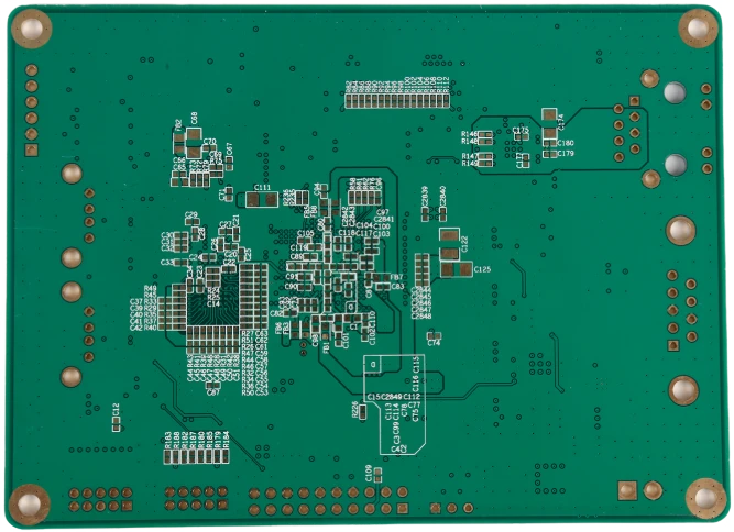
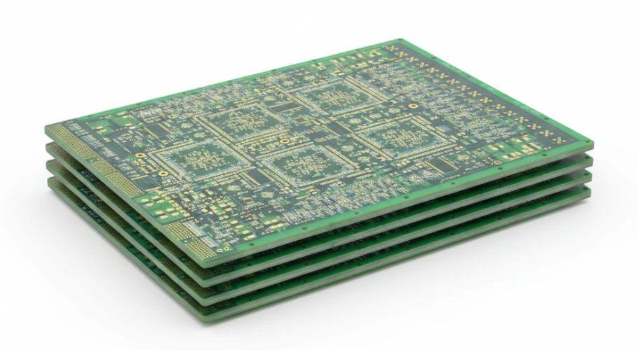
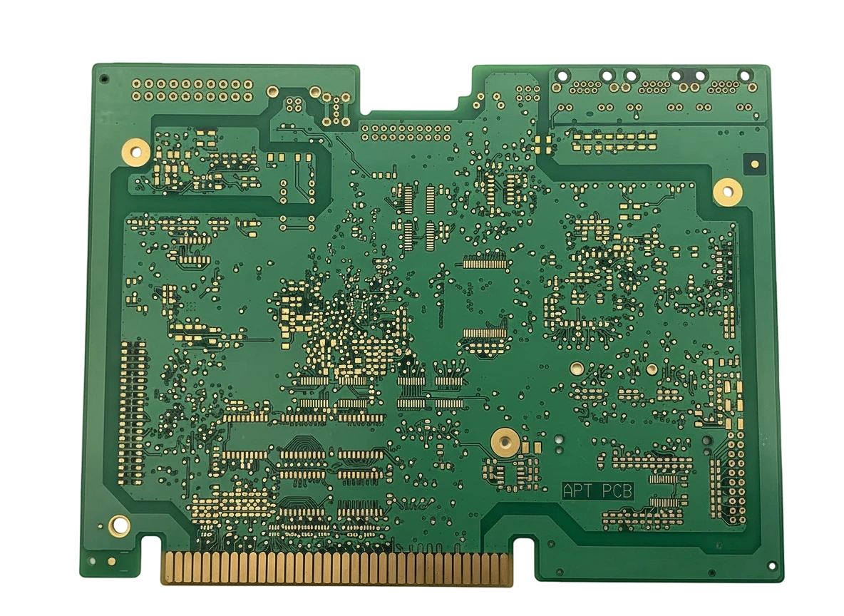
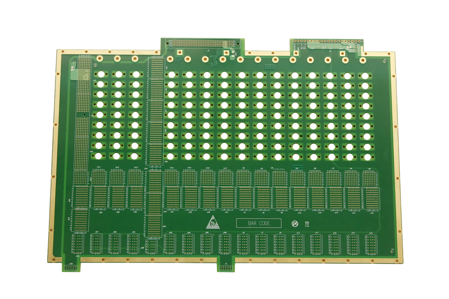
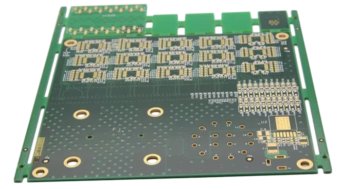
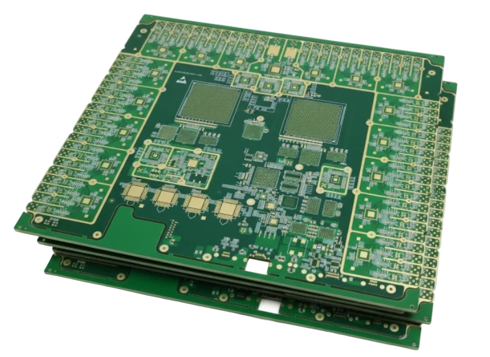
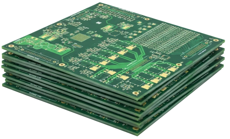
High-Tg CAM & Stackup Engineering

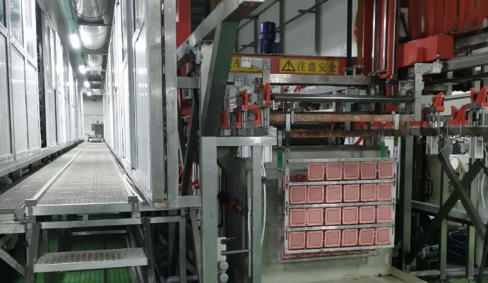
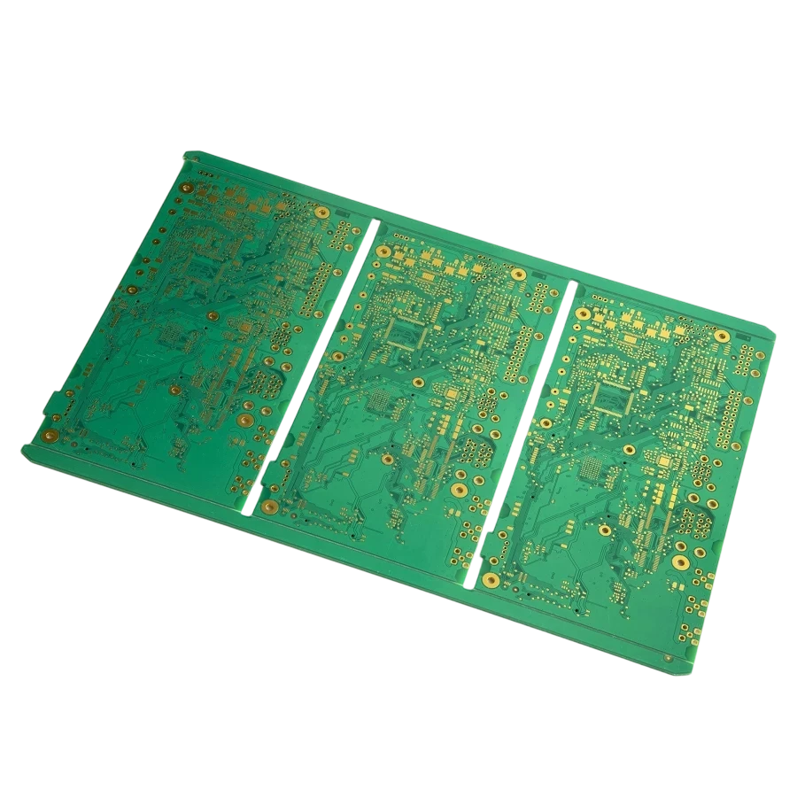
CAM engineers optimize copper balance, drill tolerances, and lamination cycles for high-Tg builds.

  • Confirm Tg/Td specs per layer and acceptable substitutes.
  • Define lamination cycles and cool-down rates to avoid resin stress.
  • Plan CAF mitigation spacing and resin-filled via usage.
  • Document bake requirements before imaging or assembly.
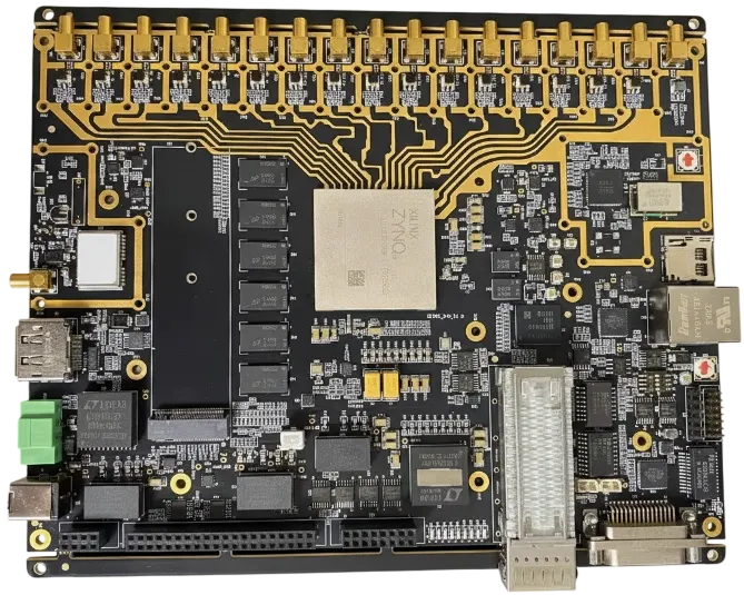
  • Specify surface finish compatible with lead-free reflow and press-fit hardware.
  • Provide coating/mask keep-outs for high-voltage areas.
  • Release packaging instructions to protect boards after baking.

Manufacturing Execution & Feedback

Process teams monitor lamination, drilling, and plating with SPC and feed results back to design.

  • Verify lamination temperature profiles and record per lot.
  • Inspect for delamination, voids, and resin starvation via cross-sections.
  • Measure drill hole quality and plating thickness.
  • Bake boards prior to finish/assembly to remove moisture.
  • Run thermal shock or T260/T288 tests as required.
  • Archive electrical, impedance, and CAF test data.
Tg 170–200°C

Material Range

S1000H, TU-872, I-Speed, etc.

≤2.8 ppm/°C

Z-Axis CTE

Controls expansion for BGAs

CAF Tested

Reliability

Per customer request

Class 3

Quality Level

IPC-6012 & automotive ready

Advantages of High-Tg PCBs

Survive higher temperatures and harsh duty cycles.

Thermal Reliability

Withstand repeated lead-free reflow and high ambient temps.

CAF Resistance

Low-CTE, high-resin systems mitigate conductive anodic filament issues.

Dimensional Stability

Tight registration for BGAs and fine-pitch connectors.

HDI Compatible

High-Tg HDI stackups support microvias and backdrill.

Lower System Cost

Reduce metal cores or mechanical supports by using robust laminates.

Qualification Support

Full test data packages for automotive, industrial, and aerospace audits.

Why Choose APTPCB?

High-Tg materials keep dimensional stability, protect vias, and extend product life in demanding environments.

AutomotiveIndustrialTelecomAerospacePower controlMedical
APTPCB production line
High-Tg lamination lines

High-Tg PCB Applications

Electronics that face continuous heat, rapid thermal cycling, or harsh environments.

Automotive ECUs, industrial drives, telecom gear, aerospace avionics, and medical imaging all rely on high-Tg boards.

Automotive & EV

ECUs, ADAS, battery management, and charging systems.

ECUADASBMSOBCLED lighting

Industrial Automation

Robotics, factory control, and power modules exposed to heat.

RoboticsDrivesPLCPower modulesUPS

Telecom & Network

Baseband, radio, and backhaul cards running hot 24/7.

BasebandRRUBackhaulSwitchesRouters

Aerospace & Defense

Avionics, mission computers, and radar controllers.

AvionicsMission computerRadarEWSatcom

Data Center & Power

Server power cards and data center controls with high thermal loads.

Server PSUDatacenter controlEdge compute

Medical & Imaging

Diagnostic equipment subjected to sterilization or continuous use.

ImagingDiagnosticsTreatmentWearables

Rigid-Flex High-Tg

Aerospace and industrial harnesses mixing rigid high-Tg cores with flex tails.

Rigid-flexHarnessEdge devices

Test & Measurement

Instrumentation subject to high dissipation and continous operation.

InstrumentationATEMeteringLab equipment

High-Tg Design Challenges & Solutions

Prevent delamination, CAF, and warpage while keeping routing density and cost under control.

Common Design Challenges

01

Material Availability

Premium Tg 200°C laminates have long lead times if not planned.

02

Warpage Control

Unbalanced copper or dielectric thickness causes bow/twist.

03

CAF Risk

Dense vias plus humidity can create conductive anodic filaments.

04

Lead-Free Assembly Stress

Multiple reflow cycles can crack poorly filled vias.

05

Thermal Expansion Mismatch

Mismatch between components and laminate strains solder joints.

06

Cost Management

Over-specifying Tg inflates BOM without added benefit.

Our Engineering Solutions

01

Material Planning

We reserve laminate lots and document acceptable alternates.

02

Copper Balancing

CAM applies cross-hatching and pours to keep layers symmetrical.

03

CAF Mitigation

Increased spacing, resin-filled vias, and bake schedules counter CAF.

04

Reflow Simulation

Thermal stress testing ensures vias survive lead-free profiles.

05

Cost-Adjusted Stackups

Recommend Tg tiers per product zone to avoid overspend.

How to Control High-Tg PCB Cost

Reserve the highest Tg materials for zones that truly require them; mix Tg tiers elsewhere. Reuse qualified stackups and panel sizes so quoting and procurement stay fast. Provide thermal targets, operating profiles, and assembly details with your data package so we can propose the most efficient construction.

01 / 08

Tiered Materials

Use Tg 180°C for hot zones and Tg 170°C elsewhere to balance cost.

02 / 08

Surface Finish Alignment

Select ENIG, OSP, or immersion silver based on assembly path.

03 / 08

Material Forecasting

Reserve laminate lots for multi-build programs.

04 / 08

Panel Optimization

Share panel tooling with related products.

05 / 08

Bake & Handling Plans

Document bake cycles to avoid unplanned rework.

06 / 08

Early DFx Reviews

Joint reviews catch warpage or CAF risks before release.

07 / 08

Standardize Vias

Keep drill sizes consistent to reduce tooling changes.

08 / 08

Coating Strategy

Define conformal coat keep-outs early to eliminate respins.

Certifications & Standards

Quality, environmental, and industry credentials supporting reliable manufacturing.

Certification
ISO 9001:2015

Quality management for high-Tg fabrication.

Certification
ISO 14001:2015

Environmental controls for lamination and plating.

Certification
ISO 13485:2016

Traceability for medical and instrumentation builds.

Certification
IATF 16949

Automotive APQP/PPAP for power electronics.

Certification
AS9100

Aerospace governance for high-temperature electronics.

Certification
IPC-6012 / 6016

Performance standards for high-reliability rigid boards.

Certification
UL 94 V-0 / UL 796

Flammability and dielectric safety compliance.

Certification
RoHS / REACH

Hazardous substance compliance.

Selecting a High-Tg Manufacturing Partner

  • Material sourcing agreements for Tg 170/180/200 laminates.
  • Documented lamination/bake cycles for high-Tg builds.
  • CAF, thermal shock, and lead-free reflow testing in-house.
  • Cleanroom SMT and coating capability.
  • 24-hour DFx response with bilingual engineers.
  • Traceability and PPAP-ready documentation for automotive customers.
Selecting a High-Tg Manufacturing Partner

Quality & Cost Console

Process & Reliability Controls + Economic Levers

Unified dashboard connecting HDI quality checkpoints with the economic levers that compress cost.

Process & Reliability

Pre-Lamination Controls

Stack-Up Validation

  • Panel utilization+5–8%
  • Stack-up simulation±2% thickness
  • VIPPO planningPer lot
  • Material bake110 °C vacuum

Pre-Lamination Strategy

• Rotate outlines, mirror flex tails

• Share coupons across programs

• Reclaim 5-8% panel area

Registration

Laser & Metrology

Registration

  • Laser drill accuracy±12 μm
  • Microvia aspect ratio≤ 1:1
  • Coverlay alignment±0.05 mm
  • AOI overlaySPC logged

Laser Metrology

• Online laser capture

• ±0.05 mm tolerance band

• Auto-logged to SPC

Testing

Electrical & Reliability

Testing

  • Impedance & TDR±5% tolerance
  • Insertion lossLow-loss verified
  • Skew testingDifferential pairs
  • Microvia reliability> 1000 cycles

Electrical Test

• TDR coupons per panel

• IPC-6013 Class 3

• Force-resistance drift logged

Integration

Assembly Interfaces

Integration

  • Cleanroom SMTCarrier + ESD
  • Moisture control≤ 0.1% RH
  • Selective materialsLCP / low Df only where needed
  • ECN governanceVersion-controlled

Assembly Controls

• Nitrogen reflow

• Inline plasma clean

• 48h logistics consolidation

Architecture

Stack-Up Economics

Architecture

  • Lamination cyclesOptimize 1+N+1/2+N+2
  • Hybrid materialsLow-loss where required
  • Copper weightsMix 0.5/1 oz strategically
  • BOM alignmentStandard cores first

Cost Strategy

• Balance cost vs performance

• Standardize on common cores

• Low-loss only on RF layers

Microvia Planning

Via Strategy

Microvia Planning

  • Staggered over stacked-18% cost
  • Backdrill sharingCommon depths
  • Buried via reuseAcross nets
  • Fill specificationOnly for VIPPO

Via Cost Savings

• Avoid stacked microvias

• Share backdrill tools

• Minimize fill costs

Utilization

Panel Efficiency

Utilization

  • Outline rotation+4–6% yield
  • Shared couponsMulti-program
  • Coupon placementEdge pooled
  • Tooling commonalityPanel families

Panel Optimization

• Rotate for nesting efficiency

• Share test coupons

• Standardize tooling

Execution

Supply Chain & Coating

Execution

  • Material poolingMonthly ladder
  • Dual-source PPAPPre-qualified
  • Selective finishENIG / OSP mix
  • Logistics lanes48 h consolidation

Supply Chain Levers

• Pool low-loss material

• Dual-source laminates

• Match finish to need

High-Tg PCB Manufacturing — Upload Data for Thermal Review

IPC Class 3 & automotive ready
High-Tg material expertise
Balanced stackup guidance
Thermal stress validation

Share stackups, Tg targets, and environment requirements—our team replies with DFx notes, lead time, and cost within one business day.

High-Tg PCB FAQ

Answers about materials, testing, and assembly for high-temperature designs.