Server and data center PCB assembly with compute, memory and high-speed connectors

Release-ready server hardware

Server & Data Center PCB Manufacturing

A server or data center PCB is a board for compute, storage, networking, power or management hardware whose stackup, high-speed channels, power delivery, thermal interfaces and test coverage must be released as one manufacturing system. This page helps hardware teams prepare the evidence needed for a viable RFQ, pilot build and production transfer.

Get an Instant Quote

Stackup + loss budgetConstruction input
SerDes + impedanceChannel input
PDN + current pathsPower input
HDI + via strategyDensity input
Backdrill definitionStub control
BOM + placement dataAssembly input
DFT + pass/fail limitsTest input
Revision + evidence planProduction input
Stackup + loss budgetConstruction input
SerDes + impedanceChannel input
PDN + current pathsPower input
HDI + via strategyDensity input
Backdrill definitionStub control
BOM + placement dataAssembly input
DFT + pass/fail limitsTest input
Revision + evidence planProduction input

What a server PCB manufacturer must resolve before production

Server and data center hardware is not one board category. A rack motherboard, NVMe backplane, network switch board, AI accelerator and power-distribution board place different demands on materials, vias, copper, connectors and test. The manufacturing package must identify the board family and its dominant release risk before a useful quote can be issued.
APTPCB reviews server and data center PCB or PCBA data as a connected set: the multilayer construction, routed interface classes, power and thermal constraints, drill and via definitions, assembly package, and inspection or test evidence. Capability, tolerances and lead time are confirmed after that review.

Start with the architecture, not a generic layer-count claim

The first decision is whether the design can use conventional through-hole multilayer construction or needs HDI structures, blind or buried vias, via-in-pad, sequential lamination or controlled-depth backdrill. The answer depends on BGA escape, routed interfaces, layer transitions, stub limits, connector fields and the final board thickness.
Material selection follows the routed channel and construction. Provide the target or approved laminate family, dielectric constraints, copper profile assumptions, impedance table and any insertion-loss limits. A low-loss label without a stackup and channel requirement cannot define a production route.

Reliability is a release discipline: failure modes and evidence

Long service life is not established by writing “24/7” on a specification. It comes from linking each failure mode to a controlled input, an inspection point and an acceptance record.
Typical failure modes and evidence:
  • Link training or margin loss: control stackup, impedance, reference-plane continuity, via transitions and residual stubs; agree coupon or measurement evidence where required.
  • Power or thermal instability: review current paths, copper distribution, thermal-via fields, component interfaces and mechanical cooling constraints; final temperature and transient validation remains at customer system level.
  • Hidden assembly defects: define paste, placement and inspection coverage for BGA, LGA, QFN and press-fit regions; use X-ray or electrical test where the package and DFT plan require it.
  • Connector or chassis mismatch: freeze datum scheme, finished-hole requirements, board outline, keepouts and mating drawings before pilot release.
  • Revision drift: align fabrication data, BOM, AVL, assembly drawing, firmware and test procedure under one approved revision.

Server motherboards: release memory, PCIe, BGA escape and PDN together

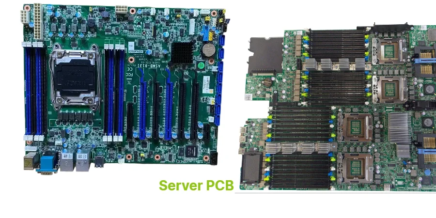
A server motherboard combines processor and memory fan-out, PCIe fabrics, management interfaces, connector fields and multi-rail power delivery. A quote needs more than Gerber files: the stackup target, impedance classes, length and skew rules, via structures, copper weights, power requirements and mechanical constraints must describe the same revision.
Call out PCIe Gen4, Gen5 or Gen6, DDR4 or DDR5, Ethernet SerDes, clocks and custom accelerator links by class. APTPCB does not infer channel constraints from net names; provide the target impedance, tolerance, reference layer, relevant loss limit and any backdrill or via-stub requirement.

Storage backplanes and midplanes: connectors and depth-controlled drilling drive risk

Storage boards combine SAS, SATA or NVMe/U.2/U.3 channels with repeated connector fields, power distribution and tight chassis datums. The release package should state the mating connector, finished-hole and press-fit requirements, entry side, layer mapping and allowed stub or backdrill geometry.
For the drilling review, separate PTH, NPTH, press-fit, blind or buried vias and backdrill groups. Provide finished dimensions and tolerances rather than only tool codes, and identify how depth, registration or residual stub will be accepted.

Network and switch boards: preserve the complete channel budget

Switch, router, line-card and fabric boards place high-speed channel design beside dense connector cages, clocks, management logic and power conversion. The RFQ should identify each SerDes family, material and copper assumptions, reference-plane transitions, connector model, routing constraints and the portion of the loss budget assigned to the PCB.
Manufacturing review can check whether the proposed stackup, trace geometry, layer changes, backdrill and fabrication tolerances are coherent. Compliance, eye margin, EMC and end-to-end channel performance remain customer system-level validation items.

AI and GPU accelerator boards: signal, power, thermal and mechanics share one envelope

AI and GPU compute boards can combine dense accelerator or FPGA packages, memory, PCIe or custom links, multi-phase power and heavy cooling hardware. BGA escape and routing density may drive HDI, but the via architecture must also leave room for current return paths, thermal transport and assembly inspection.
Provide the device package drawings, placement data, current and transient assumptions, heatsink or cold-plate datums, keepouts, board support points and test access strategy. Final power integrity, thermal performance and accelerator operation must be validated in the customer’s assembled system.

Power and distribution boards: define current paths and safety boundaries

Server power, distribution and control boards require explicit operating voltage, current by rail, copper-weight intent, connector ratings, thermal interfaces, isolation boundaries and protection architecture. Trace width or copper weight cannot be selected from total system power alone.
State the applicable product and safety requirements, creepage or clearance constraints, hipot or functional-test limits and mechanical cooling conditions. PCB and PCBA manufacturing evidence supports the customer’s qualification, but final electrical safety and system compliance remain the customer’s responsibility.

Signal-integrity release: five inputs must agree

Release these five input sets together:
  • Interface class: protocol or custom link, data-rate class, topology and receiver or transmitter assumptions.
  • Stackup: dielectric construction, copper profile, finished thickness and reference layers.
  • Geometry: impedance target and tolerance, width and spacing intent, length or skew rule and breakout constraints.
  • Transitions: via layers, pad and antipad intent, backdrill entry and residual-stub target where used.
  • Evidence: coupon, TDR, insertion-loss or other acceptance method when required by the customer specification.
Changing one input after routing may invalidate the others. Record approved deviations and update the fabrication drawing, stackup, impedance table and design data under the same revision.

Build a test ladder from bare board to functional acceptance

The inspection plan should follow the risks of the board family. Bare-board electrical test, impedance coupons, dimensional inspection or microsection can be specified for fabrication. Assembly coverage may add SPI, AOI, X-ray, ICT, flying probe or functional testing as applicable.
ICT and FCT are not generic checkboxes. The customer must provide DFT access, fixtures or fixture responsibility, firmware, power-up sequence, loads, interface setup, expected outputs and objective pass or fail limits. Pilot evidence should be reviewed before the production test flow is frozen.

Board-family decision matrix: dominant risk and RFQ evidence

Server motherboard

Dominant risk: BGA escape, memory and PCIe timing, PDN and dense mechanics. RFQ evidence: stackup, interface-class table, via strategy, power inputs and connector drawings.
Storage backplane or midplane

Dominant risk: repeated high-speed channels, press-fit geometry and residual stubs. RFQ evidence: connector specification, drill table, layer mapping, backdrill definition and chassis datums.

Network or switch board

Dominant risk: channel loss, crosstalk, reference transitions and cage alignment. RFQ evidence: loss allocation, impedance table, material assumptions, via transitions and connector models.

AI or GPU accelerator

Dominant risk: dense fan-out, transient current, heat flow and heavy cooling hardware. RFQ evidence: package data, HDI structure, rail currents, thermal and mechanical datums, and DFT plan.

Power or distribution board

Dominant risk: current density, temperature rise, isolation and connector heating. RFQ evidence: voltage and current by rail, copper intent, safety boundaries, cooling conditions and test limits.

Management, riser or control board

Dominant risk: mixed-signal interfaces, mating geometry, revision drift and incomplete functional coverage. RFQ evidence: interface list, mating drawings, BOM/AVL, firmware and acceptance procedure.

Server PCB RFQ, pilot and production release gates

RFQ gate:
  • Fabrication data, drill files, drawing, stackup and impedance or loss requirements share one revision.
  • Board family, layer count target, materials, copper, via and backdrill structures, connector constraints and quantities are stated.
  • BOM/AVL, placement and assembly drawings, test requirements and forecast volumes are included for PCBA.
Pilot release:
  • DFM questions and approved deviations are closed in writing.
  • Coupon, dimensional, microsection, X-ray, electrical and functional evidence is assigned to the relevant risk.
  • Fixtures, firmware, loads and pass/fail limits are ready for the tests required on pilot units.
Production release:
  • First-article evidence is accepted and the fabrication, BOM, AVL, assembly and test revisions are frozen.
  • Change control, lot traceability, inspection records and packaging requirements are agreed.
  • Volume, panel or assembly assumptions and material availability are rechecked before scheduling.
Release-hold criteria: unresolved layer mapping, ambiguous finished-hole or via data, missing channel requirements, connector or chassis conflicts, unapproved substitutions, and absent test limits remain holds. Capability, tolerance, lead time and evidence are confirmed only after these items are resolved.

What buyers should receive from an APTPCB technical review

A useful manufacturing review converts the design package into explicit decisions: proposed construction, open assumptions, DFM conflicts, required customer inputs, inspection or test evidence, and the points that must be closed before pilot or production release.
APTPCB reviews the supplied PCB and PCBA data against the requested board family and build stage. The response can then distinguish what is confirmed, what is conditional on customer data, and what remains a release hold, giving engineering and procurement a clearer basis for comparison and change control.

Request a server or data center PCB manufacturing review

Send the current design revision, stackup, interface and impedance table, drill or via notes, BOM and test requirements. APTPCB can review the package before confirming the manufacturing route, evidence plan and quote.

Frequently Asked Questions

What makes a server or data center PCB different from a standard industrial PCB?

A server or data center PCB often combines dense BGA escape, multiple high-speed interface classes, high-current power delivery, tight mechanical envelopes and a larger test burden. Manufacturability depends on the complete stackup, via strategy, impedance and loss targets, connector rules, thermal constraints and evidence plan, not on layer count alone.

Which server and data center board families can be reviewed for manufacturing?

The review can cover server motherboards, storage backplanes and midplanes, network and switch boards, AI or GPU accelerator boards, power and distribution boards, and management, riser or control boards. The manufacturing route is confirmed only after APTPCB reviews the actual design package and requirements.

What data should be included in a server PCB RFQ?

Provide ODB++ or Gerber data, drill files, fabrication drawing, final or target stackup, impedance and loss requirements, via and backdrill notes, board outline and connector tolerances, BOM with approved sources, placement data, assembly drawing, test specification, forecast volumes and revision status.

How should materials be selected for a server or AI compute PCB?

Material selection should start from the channel loss budget, dielectric thickness, copper profile, thermal requirements, lamination structure and supply constraints. A low-loss product name by itself is not a release criterion; the proposed construction must be checked against the routed interfaces and production stackup.

When are HDI, blind or buried vias, VIPPO or backdrill needed?

These structures are considered when BGA escape, routing density, connector geometry or via-stub limits cannot be met with ordinary through vias. State the connected layers, finished geometry, fill or cap requirement, residual stub target and inspection method so the via route can be reviewed.

Which tests should be defined for a server PCBA?

The test plan may combine bare-board electrical test, impedance coupons when specified, SPI, AOI, X-ray for hidden joints, ICT or flying probe, and functional test. ICT and FCT require suitable DFT access, fixtures, firmware, procedures and objective pass or fail limits from the customer.

When are capability, tolerance, lead time and production evidence confirmed?

Capability, manufacturing tolerances, lead time and the evidence package are confirmed after technical review of the complete files, material construction, via strategy, assembly risks, test inputs, volume and revision controls. Unresolved assumptions remain release holds rather than being converted into fixed promises.