Quality Assurance

AOI Optical Inspection for PCB & PCBA

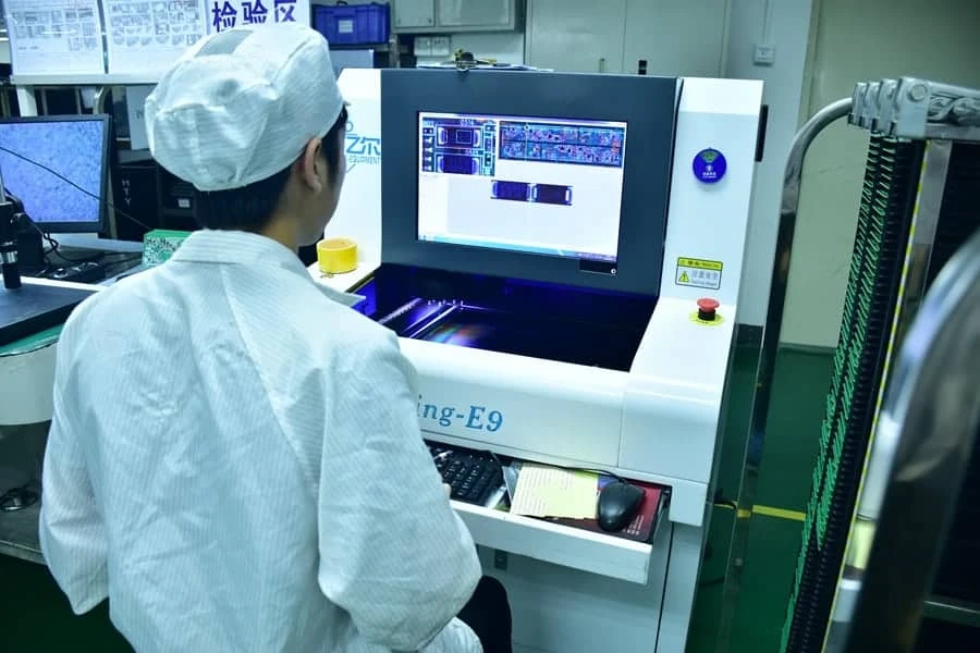
Automated Optical Inspection is critical for detecting defects on bare PCBs and assembled boards. APTPCB deploys advanced 2D/3D AOI technology throughout fabrication and assembly to catch issues early, reduce escapes, and ensure superior product quality.

Get an Instant Quote

Full Quote →
Advanced Detection2D & 3D AOI
<100 ppmDefect Escape Rate
100% InlineCoverage
SPI + X-Ray + ICTIntegration

AOI Optical Inspection: Ensuring Superior Quality for Bare PCBs and PCBA

In electronics manufacturing, the quality of PCBs and PCBA forms the foundation of product performance and reliability. Any hidden defect at the board level can escalate into field failures, costly returns, and reputational damage.
APTPCB fully integrates AOI technology as an indispensable component of our comprehensive quality management system. By combining advanced 2D/3D AOI, robust programming, and data-driven process feedback, we help you catch defects as early as possible, reduce defect escapes to downstream stages and customers, improve first-pass yield (FPY), and support long-term reliability in demanding applications.

Bare PCB AOI Test: Laying the Foundation for PCB Quality

During the bare PCB manufacturing phase, AOI testing is a pivotal step in verifying the integrity of the finished conductor trace image. It meticulously compares the fabricated board against the original Gerber data, identifying deviations that even Electrical Tests (E-Tests) might overlook.
Unlike E-Tests, which primarily check continuity and isolation, bare board AOI focuses on geometric and visual accuracy of every trace, pad, and plane. AOI can detect conductor traces that are narrowed but still unbroken—a subtle defect an E-Test would miss. If left unaddressed, such imperfections can severely compromise product performance, current-carrying capacity, signal integrity, and long-term reliability.
Typical issues detected by Bare PCB AOI include:
  • Narrowed or over-etched traces that alter impedance or reduce current capacity
  • Copper slivers, bridges, or residues that can become latent shorts
  • Insufficient annular ring, broken pads, or irregular pad shapes
  • Localized copper missing or excess in critical areas
  • Etching or plating anomalies that affect reliability
Critical Applications for Bare PCB AOI:
  • High-Frequency Circuits: Ensuring precise trace impedance, consistent line width/spacing, and optimal signal integrity in RF and high-speed designs.
  • High Power Loads: Verifying adequate copper width and uniformity for robust current-carrying capacity and effective heat dissipation.
  • High Data Transmission Rates: Guaranteeing uniform trace dimensions and layer registration for consistent signal propagation and minimal crosstalk.
  • Sensitive Analog Circuits: Preventing subtle trace defects and contamination that could introduce leakage paths or unwanted noise.
For multilayer PCBs, AOI plays an indispensable role. Inner layers are meticulously scanned by AOI before lamination, catching defects such as opens, shorts, misalignment, or pattern irregularities that would otherwise be permanently embedded and undetectable after pressing.

SMT AOI Test: Guaranteeing Flawless Assembly Processes

In SMT PCB assembly, AOI stands as a paramount testing methodology. While bare board AOI secures the copper image, SMT AOI ensures that every component is placed and soldered correctly on that image—before boards move to downstream testing or system integration.
Our advanced AOI machines capture high-resolution images of assembled PCBAs and leverage sophisticated image processing software to compare these against a 'golden board' reference or a program generated from CAD/BOM data. This systematic comparison enables us to precisely identify even the most subtle defects.
The Core Detection Process Encompasses:
  • Image Capture: Strategically mounted color or black/white cameras positioned above the board with angled and multi-directional lighting to detect subtle height variations and solder shapes. Automatic board conveyance ensures 100% coverage of the entire assembly.
  • Image Analysis: Specialized software rigorously compares captured images against the golden board or CAD-derived reference. Advanced image processing algorithms detect anomalies in presence, position, orientation, polarity, and solder quality.
  • Results & Reporting: Precise defect location coordinates (X/Y, reference designator) and size data. Detailed images or video snippets of detected flaws for review and documentation. Comprehensive reports including defect classifications, failure statistics, and Pareto charts.

Defect Types Detected by APTPCB's AOI

APTPCB's AOI inspection is highly effective in identifying a broad spectrum of assembly-related defects, systematically categorized as follows:
Component Flaws:
  • Missing or extra components
  • Incorrect or misloaded parts (value/package mismatches)
  • Shifted, skewed, or misaligned components
  • Incorrect orientation or reversed polarity
  • Tombstoned, flipped, or standing components
Solder Joint Issues:
  • Insufficient solder, risking opens or weak joints
  • Excessive solder, risking bridging or long-term reliability concerns
  • Solder balls and splatter on the board surface
  • Solder bridging between pads or fine-pitch leads
  • Solder voiding and abnormal joint shape
PCB Defects & Contamination:
  • Trace damage, scratches, or exposed copper caused during handling or assembly
  • Hole plugging, pad lifting, or localized plating defects
  • Foreign object debris (FOD) on or near critical areas
  • Residual flux or contamination visible at critical joints
  • Missing silkscreen print or misaligned legends

2D vs. 3D AOI Technology: APTPCB's Advanced Options

The evolution of AOI technology offers varying levels of inspection depth and capability. APTPCB strategically deploys both 2D and 3D AOI, with a preference for advanced solutions where product risk and complexity demand it.
2D AOI: A cost-effective inspection solution using single-angle or near single-angle imaging. Well-suited for verifying component presence, position, orientation, and basic solder appearance. Ideal for less complex boards or where solder volume and height are not critical risk drivers.
3D AOI: Captures multi-angle images and constructs a detailed 3D height map of the circuit board. Provides accurate measurements of solder paste or solder joint volume, height, and shape. Detects a wider range of defects including lifted leads, floating components, marginal solder insufficiency, and coplanarity issues. Particularly powerful for BGA, QFN, fine-pitch ICs, and dense assemblies where height-related defects are critical.
APTPCB prioritizes and deploys 3D AOI for critical assemblies and high-reliability applications, while combining it with 2D AOI where it delivers the best cost-performance balance.

APTPCB's AOI Inspection Process and Strategy

APTPCB's AOI inspection process is meticulously engineered to deliver systematic and robust quality assurance, integrating seamlessly into our production workflow. We treat AOI as both a quality gate and a process feedback tool.
Our AOI Inspection Process Steps:
  • Setup & Programming: We meticulously program the inspection routine by importing CAD/Gerber/BOM data or validated golden board images, defining inspection regions for components, pads, polarity marks, and critical areas, and optimizing lighting, cameras, and focus for each product family.
  • Settings Verification: Sample boards are tested to fine-tune defect detection thresholds and inspection windows, adjust for real-world component and process variation, and confirm accurate failure calls with minimal missed defects.
  • Production Testing: During mass production, AOI is integrated for automatic board handling and scanning with continuous, inline operation, immediate pass/fail indication and board segregation when necessary, and real-time process monitoring and trend analysis.
  • Failure Review: Detected failure images and coordinates are reviewed by trained personnel. Boards with critical defects are rejected or routed for repair according to product class. Faults are categorized by type, severity, and location.
  • Reporting & Analysis: Comprehensive reports detailing failure rates, defect distribution, and top recurring issues are generated. Failure patterns and trends are identified at the component, design, and process levels. Root cause analysis is performed in collaboration with process and design teams.

APTPCB's AOI Equipment Configurations

APTPCB deploys a range of AOI equipment configurations, each tailored to meet diverse production demands and ensure optimal efficiency:
Inline AOI: Directly integrated into the SMT production line. Inspects boards immediately after critical process steps (commonly post-reflow). Provides the fastest defect detection at the source, ideal for medium to high volumes.
Standalone AOI: Flexible off-line operation for sampling, audits, and engineering builds. Typically used to verify process quality, support NPI (New Product Introduction), and troubleshoot issues. Enables detailed analysis without impacting line throughput.
Dual Lane AOI: Features two independent inspection lanes within a single system. Effectively doubles throughput capacity for high-volume production. Offers redundancy and flexible line balancing options.

Reducing False Calls: APTPCB's Optimization Strategies

False calls—where the AOI system incorrectly reports a defect—can significantly impact production efficiency and operator trust. APTPCB employs a multi-faceted approach to minimize these occurrences:
  • Optimizing lighting, focus, thresholds, and algorithms for each product family
  • Enriching the 'golden board' reference with all acceptable variations
  • Marking acceptable design features and cosmetic variations as permissible exceptions
  • Training AOI programs with representative production samples, not just ideal prototypes
  • Performing regular maintenance and calibration to maintain peak optical performance
  • Tuning detection parameters dynamically based on historical inspection and FPY data
  • Thoroughly reviewing detected calls before final board rejection, and feeding confirmed false calls back into program refinement
Through these measures, AOI at APTPCB functions as a reliable decision tool, not just an alarm generator.

AOI Integration with Other Test Methods

While AOI technology is profoundly powerful, it possesses inherent limitations. APTPCB strategically integrates AOI with other advanced inspection and test methods to provide a truly comprehensive and robust layered quality assurance framework.
AOI vs. ICT (In-Circuit Test): AOI primarily identifies assembly flaws through visual and geometric analysis. ICT performs electrical tests at the node level to verify continuity, shorts, component values, and some functional parameters. AOI can be applied earlier in the process, right after reflow, to prevent defective boards from reaching ICT. ICT then validates electrical performance on boards that have already passed the visual and geometric gate.
AOI vs. X-Ray: AOI is generally lower cost and faster with higher throughput for inline inspection. X-ray inspection excels at revealing subsurface and hidden defects, such as voids in BGA or bottom-terminated component joints, hidden bridges under packages, and internal shorts. APTPCB uses AOI as the primary high-throughput tool and deploys X-ray selectively for critical components, complex packages, or process validation.
AOI vs. SPI (Solder Paste Inspection): AOI inspects the assembly after reflow, evaluating solder joint formation, wetting, and component placement. SPI checks solder paste print quality before component placement and reflow, ensuring correct paste volume, height, and alignment. Together, SPI and AOI form a closed loop: SPI prevents many solder-related issues from occurring, and AOI verifies the final result on the finished assembly.

Key Benefits of APTPCB's AOI Services

Early Defect Detection

Catch defects at the source—bare board or post-reflow—before they propagate downstream.

Reduced Escape Rate

Systematic inspection keeps defect escapes below 100 ppm, protecting your reputation and reducing warranty costs.

Improved First-Pass Yield

Real-time process feedback and corrective actions enhance FPY and shorten debug cycles.

Data-Driven Insights

Comprehensive defect reports, Pareto charts, and trend analysis drive continuous process improvement.

Cost-Effective Quality

Strategic deployment of 2D/3D AOI balances inspection rigor with production efficiency.

Integrated Quality System

AOI seamlessly integrates with SPI, X-ray, ICT, and functional testing for comprehensive coverage.

Why Partner with APTPCB for AOI Inspection Services

APTPCB's AOI services are backed by decades of manufacturing expertise, advanced equipment, and a commitment to continuous improvement. We understand that AOI is not just a checkpoint—it is a strategic tool for achieving superior product quality and operational efficiency.
Our thorough understanding of AOI's capabilities, combined with a keen awareness of factors such as false calls and inherent limitations, empowers our manufacturing engineers to optimally apply AOI as a vital component of a comprehensive quality strategy. Through APTPCB's effective implementation, AOI furnishes invaluable inspection data to drive process improvement, yield and first-pass yield are significantly enhanced, defective product escapes are dramatically reduced, and consistent, high-level product quality is achieved and sustained.

Enhance Your PCB & PCBA Quality with AOI Inspection

Share your product specifications, volume requirements, and quality objectives. Our quality engineers will recommend the optimal AOI strategy—2D, 3D, inline, or standalone—tailored to your needs.