HDI PROGRAM

HDI PCB Manufacturing — Faster, Smarter, More Cost-Effective

APTPCB provides high-density interconnect PCBs with optimized stack-ups, fast turnaround, and cost-efficient microvia technology for next-generation electronics.

  • Optimized Stack-Up Design
  • High-Yield Microvia Process
  • Cost-Effective HDI
  • Fast Turnaround
  • Precision Impedance
  • DFM Support

Get an Instant Quote

Full Quote →

HDI PCB One-Stop Manufacturing and Assembly Service

APTPCB provides comprehensive one-stop HDI PCB manufacturing and assembly services — from advanced PCB fabrication to full turnkey assembly. Our HDI solutions are engineered for high-density interconnection, enabling miniaturized, high-speed, and high-reliability electronic designs.

We specialize in precision laser microvia drilling, sequential lamination, fine-line imaging, and high-layer-count stack-ups (1+N+1, 2+N+2, Any-Layer HDI). These technologies ensure superior electrical performance, signal integrity, and space utilization for compact devices and complex systems.

Backed by integrated engineering support and rigorous quality control, APTPCB streamlines your HDI project from prototype to volume production — reducing costs, accelerating time-to-market, and ensuring stable performance for every board.

APTPCB's HDI field data confirms the immediate gains from our program—30–70% smaller outlines, shorter routing for higher signal integrity, microvia reliability, and system-level cost reductions through smaller enclosures and simplified assembly. We embed that ROI model into front-end feasibility reviews so customers know exactly when HDI delivers value.

Our internal stack-up library catalogs 1+N+1, 2+N+2, and 3+N+3+ any-layer architectures plus their target industries (consumer, ADAS, high-compute, 5G, aerospace, medical). We reuse that taxonomy to lock materials, lamination cycles, and via templates for every configuration.

HDI manufacturing line

HDI PCB Solutions We Delivered

A snapshot of our manufacturing and assembly capabilities across industries.

Circuit Board Manufacturing

Circuit Board Manufacturing

PCB Assembly Services

PCB Assembly Services

Electronic Circuit Design

Electronic Circuit Design

Microelectronics Solutions

Microelectronics Solutions

Defense & Aerospace

Defense & Aerospace

High-Speed Computing

High-Speed Computing

High-Quality HDI PCB Manufacturer

From fine-line imaging and laser microvias to via-in-pad and any-layer ELIC, APTPCB delivers tight impedance, high reliability, and on-time builds for smartphones, RF modules, automotive electronics, and AI/5G systems.

Download Capabilities
Any-Layer ELIC ProductionMicrovia Reliability: Stacked vs Staggered±5% Impedance ControlPCIe/SerDes BackdrillMegtron 6/7 • Rogers 4350BEV/ADAS • AI • 5G

APTPCB HDI PCB Manufacturing Services

APTPCB provides complete HDI (High-Density Interconnect) PCB manufacturing solutions from light to complex multilayer structures. Our HDI boards are engineered with microvias, fine lines, and sequential lamination to achieve compact, high-performance interconnections for advanced electronics such as smartphones, RF modules, and industrial control systems.

HDI PCB Types We Offer

HDI PCB stack-ups are categorized by the number of sequential buildup (SBU) layers added to the core. The notation X + N + X indicates buildup layers on each side (X) and core layers (N). APTPCB supports all HDI configurations for different density and reliability requirements.

  • 1 + N + 1 (Type I HDI) – One buildup layer on each side, single-layer microvias. Ideal for moderate I/O density designs and cost-sensitive applications.
  • 2 + N + 2 (Type II HDI) – Two buildup layers per side, combining microvias and buried vias. Provides higher routing density for fine-pitch BGAs.
  • 3 + N + 3 (Type III HDI) – Three or more buildup layers per side with stacked microvias. Used in high-end mobile, RF, and computing products.
  • Mixed or Asymmetric Structures (e.g., 1 + N + 2, 2 + N + 3) – Customized hybrid stack-ups for specific design and signal integrity needs.

Via and Interconnect Structures

  • Through-Hole Via: Traditional via passing through the entire PCB, economical for simple interconnections.
  • Blind Via: Connects an outer layer to one or more inner layers, saving routing space.
  • Buried Via: Located between internal layers, invisible on the outer surface.
  • Microvia: Laser-drilled via (≤0.25 mm) used for HDI layer-to-layer interconnection.
  • Via-in-Pad: Microvia placed within component pads, filled and capped to ensure flat soldering surfaces.
  • Stacked Microvia: Vertically aligned vias offering ultra-high density for compact BGA designs.
  • Staggered Microvia: Offset vias between layers, improving yield and mechanical reliability.

Typical HDI Stack-Up Examples

  • 6-Layer (1 + 4 + 1): Single buildup on each side, microvias between outer and adjacent layers; suitable for 0.65 mm BGA pitch designs.
  • 8-Layer (2 + 4 + 2): Dual buildup per side, microvia-to-buried via connections for 0.5 mm pitch BGAs.
  • 10-Layer or More (3 + N + 3): Three or more buildup layers with stacked microvias; used in high-density computing, RF, and advanced SoC applications.

Material and Design Guidelines

HDI PCBs use ultra-thin cores and prepregs (30–150 µm) to achieve low-aspect-ratio microvias. Typical copper thickness is 18–35 µm. For high-speed or RF designs, APTPCB supports low-loss materials such as Panasonic Megtron, Isola I-Speed, and Rogers laminates. All materials feature high Tg and low CTE for thermal reliability during sequential lamination.

  • Microvia diameter: 0.1–0.25 mm, aspect ratio ≤ 1:1.
  • Minimum trace/space: 3/3 mil or finer depending on capability.
  • Impedance tolerance: ±5% with controlled dielectric thickness.
  • Via-in-pad structures: Filled and capped for solderability and reliability.

Reliability and Quality Assurance

APTPCB performs 100% electrical testing, X-ray inspection, and micro-section analysis to ensure plating integrity and via reliability. Staggered microvia structures are preferred for enhanced thermal cycling endurance. Each HDI PCB undergoes reflow simulation and impedance verification before mass production.

Cost and Application Recommendations

  • 1 + N + 1: Economical solution for compact consumer electronics.
  • 2 + N + 2: Balanced choice for mobile, IoT, and wireless modules.
  • 3 + N + 3: Premium structure for advanced communication and computing systems.

HDI PCB Manufacturing Process

1

Core Preparation

Material selection, thickness control, and surface preparation to establish the foundation layer.

2

Sequential Build-Up Lamination

Multi-cycle lamination with controlled temperature and pressure to create additional layers.

3

Laser Microvia Drilling

CO₂ and UV precision laser drilling for creating microvias with extreme accuracy.

4

Microvia Metallization

Electroless copper deposition, via filling, and planarization for reliable connections.

5

Architecture Selection

Reference the stack-up catalog to choose 1+N+1/2+N+2/3+N+3 structures, dielectric thicknesses, and any-layer ELIC needs, then release material and blind/buried-via rules.

6

Microvia & Lamination Execution

Run sequential lamination, laser drilling, copper fill, and planarization per the HDI playbook to hold ±5% impedance and reliable via-in-pad.

7

Application-Level Validation

For automotive, 5G, or aerospace builds, add X-ray, cross-sections, and thermal cycling to validate the selected architecture before release.

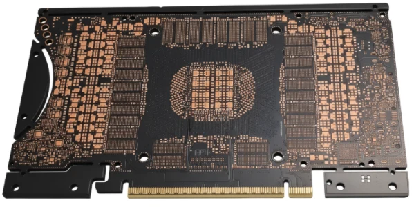
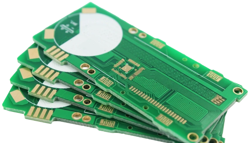
CAM Engineering Workflow — Converting Design Data into a Manufacturable HDI Process

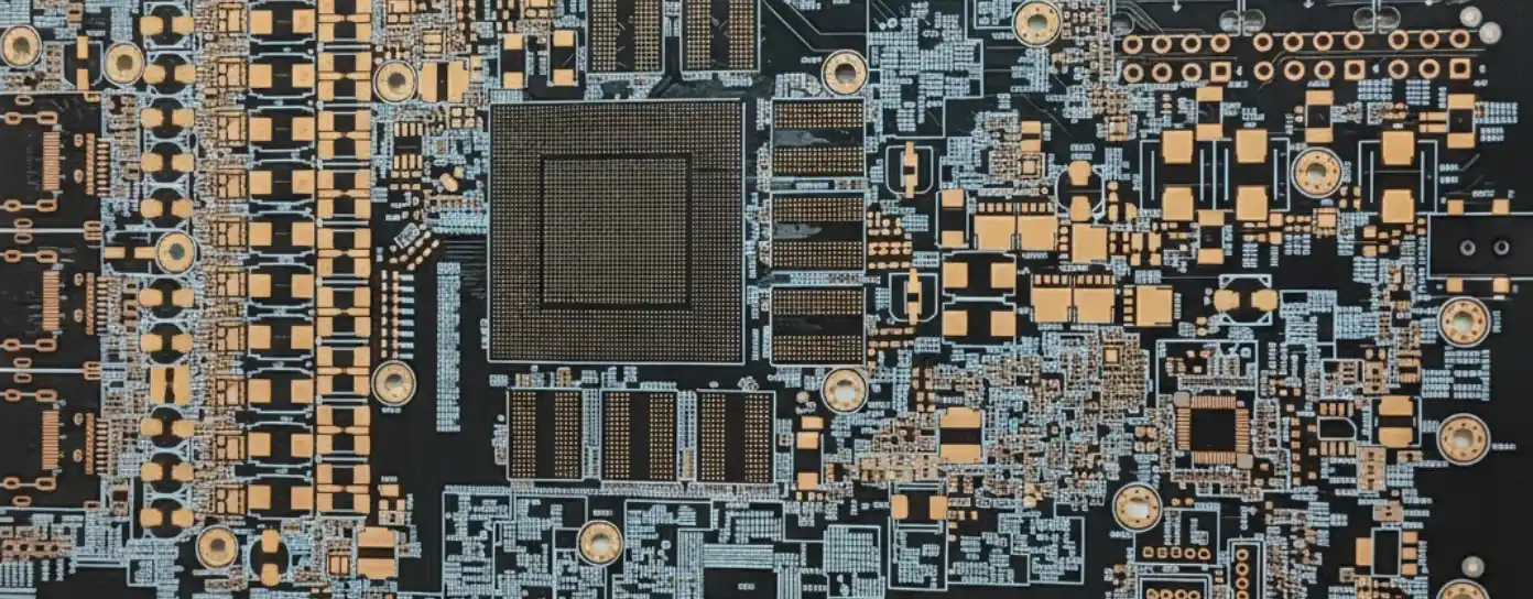
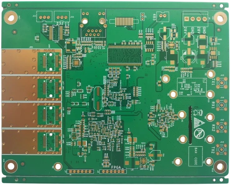
In the HDI PCB manufacturing process, the first essential phase is led by CAM engineers, who translate design intent into a precise, manufacturable production plan. After receiving Gerber or ODB++ data, they verify stack-up structures, microvia configurations, and impedance requirements. Through DFM analysis, drill programming, and fabrication note preparation, CAM engineers ensure every design feature aligns with production capabilities.

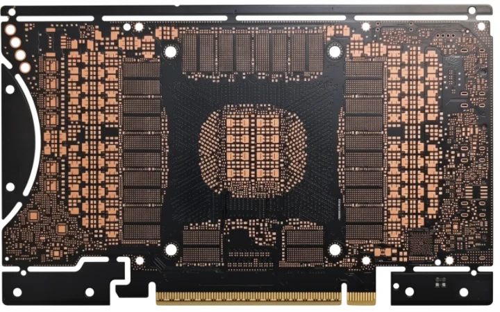
  • Validate Gerber/ODB++ and confirm HDI layer stack-up, copper thickness, and prepreg configuration.
  • Perform DFM/DFT checks — trace width and spacing, microvia pitch, annular ring size, and aspect ratio compliance.
  • Generate precision drill and laser coordinate files (UV/CO₂) for microvias, blind vias, and buried vias.
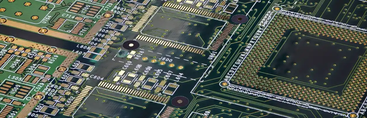
  • Annotate impedance-controlled nets, high-speed signal layers, and reference planes for fabrication accuracy.
  • Optimize panelization, fiducial placement, and tooling holes for stable lamination and imaging alignment.
  • Define fabrication notes including via-fill method, surface finish, and copper balancing requirements.
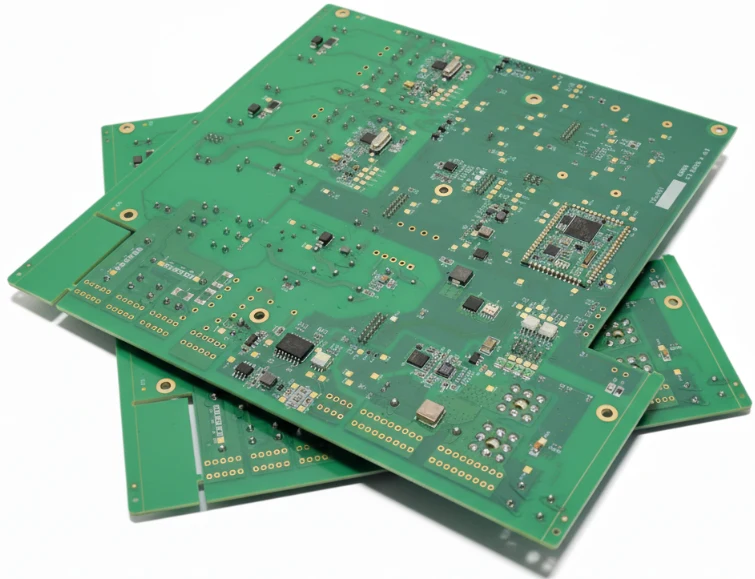
  • Collaborate with production engineers for manufacturability review and process flow validation before release.

Production Execution & Continuous Process Optimization — From Lamination to Final Inspection

On the factory floor, sequential lamination, laser drilling, copper filling, and planarization are monitored under SPC dashboards. Real-time feedback ensures every lamination cycle stays within temperature, pressure, and registration tolerances before release to assembly.

  • Control lamination temperature, pressure, and dwell time during each sequential build-up stage.
  • Monitor laser drilling focus, power, and alignment to ensure accurate and clean microvia formation.
  • Regulate electroless and electrolytic copper deposition for uniform via-fill and layer-to-layer conductivity.
  • Perform planarization and surface treatment to achieve smooth surfaces for subsequent imaging and bonding.
  • Use AOI, X-ray, and cross-section inspection to verify layer registration, via integrity, and plating quality.
  • Apply SPC and yield analysis to identify variations in lamination, drilling, or plating processes.
  • Feed process data back to CAM engineers to refine tooling, drill maps, and fabrication notes for future builds.
30-70%

Space Savings

Smaller form factor

50μm

Min Trace Width

Ultra-fine lines

150μm

Microvia Size

Precision drilling

30+

Layer Capacity

Complex designs

Advantages of HDI PCB

Why HDI is the preferred architecture for next-generation high-density electronics

Compact Form Factor

Microvias and fine-line routing enable a 30–70% smaller board footprint for thinner, lighter products.

Higher Component Density

Any-layer interconnects and via-in-pad offer more routing freedom to fit complex ICs in limited space.

Superior Electrical Performance

Shorter paths & controlled impedance reduce delay, crosstalk, and EMI—ideal for high-speed I/O & 5G RF.

Thermal & Mechanical Reliability

Balanced stack-ups, copper-filled microvias, and high-Tg laminates stay robust through multiple reflows.

Enhanced Design Flexibility

Sequential build-up unlocks dense BGA breakout without inflating total layer count.

System-Level Cost Efficiency

Smarter routing can mean fewer layers and smaller boards—lowering BOM and assembly costs at scale.

Harder to Reverse Engineer

Microvia layers, ultra-fine lines, and blind/buried links make internal tracing extremely difficult—protecting IP.

Faster Signal Paths

Short interconnects reduce latency and keep loss budgets tight for AI, RF, and automotive systems.

Why Choose APTPCB?

HDI enables higher routing density, faster signals, and better reliability in a smaller, lighter assembly — benefits conventional multilayer boards cannot match.

SmartphonesADAS / EV5G RFMedicalAerospaceAI / Servers
APTPCB production line
In-house HDI lines • IPC-2226/6016 • ISO 9001 • IATF 16949 • AS9100 • ISO 13485

HDI PCB Applications

Powering innovation across industries with advanced interconnect technology

HDI PCB technology enables miniaturization, signal integrity, and reliability for next-generation electronics — driving smarter, faster, and more connected systems across industries.

Consumer Electronics

Powering ultra-compact, high-performance devices for the modern lifestyle.

SmartphonesTabletsWearablesAR/VRGaming Consoles

Automotive Electronics

Enhancing vehicle intelligence with reliable HDI circuits for safety and power control.

ADASEV ControlsInfotainmentSensorsPower Modules

Medical Devices

Delivering precision and reliability for life-saving and diagnostic equipment.

ImplantsImagingDiagnosticsPatient MonitorsPortable Devices

Telecom & 5G

Supporting high-frequency, low-loss performance for next-generation wireless networks.

Base StationsAntennasIoT GatewaysRoutersRF Modules

Aerospace & Defense

Mission-critical reliability in extreme environments for defense and avionics systems.

AvionicsSatellitesDronesRadarCommunication Systems

Industrial & Automation

High-density PCB solutions for smart manufacturing and precision control systems.

RoboticsPLCsSensorsPower ControlIndustrial IoT

Computing & AI Hardware

Enabling high-speed, high-density interconnections for next-gen processors and servers.

AI AcceleratorsGPUsData CentersServersMemory Modules

Networking & Data Infrastructure

Delivering high-speed signal integrity for cloud and data communication equipment.

Network SwitchesRoutersOptical ModulesBackplanesEdge Computing

HDI PCB Design Challenges & Solutions

As circuit density continues to rise, HDI PCB design presents unique challenges — from microvia reliability to manufacturability control.

Common Design Challenges

01

Microvia Reliability Risks

Microvias with excessive aspect ratios or poor copper fill can crack under thermal stress, leading to intermittent opens during reflow cycles.

02

Fine-Pitch BGA Breakout Limitations

0.3–0.4 mm BGAs create dense fan-out areas where conventional through-holes are no longer viable, increasing routing congestion and layer count.

03

Stack-Up Warpage & Layer Misalignment

Multiple sequential laminations can cause dimensional shift or uneven expansion, resulting in registration errors and uneven layer bonding.

04

Signal & Power Integrity Concerns

Tight spacing, thin dielectrics, and high-speed differential pairs increase crosstalk and make impedance control more difficult.

05

Thermal Density & Material Constraints

Compact HDI layouts trap heat, while mixed dielectric materials produce different CTE rates, affecting reliability.

06

Manufacturability Gaps

Designs pushed to fab limits may violate minimum spacing, annular rings, or via-to-trace clearances, lowering yield and increasing cost.

Our Engineering Solutions

01

Controlled Microvia Geometry

All microvias are laser-drilled with an aspect ratio ≤ 1:1 and copper-filled, planarized via-in-pad construction for consistent plating and structural integrity.

02

Optimized Fan-Out Architecture

Use staggered or stacked microvia routing to achieve clean BGA breakout while minimizing lamination cycles and maintaining impedance consistency.

03

Symmetrical Stack-Up Engineering

Balanced dielectric layers and precise material selection reduce warpage and improve alignment across multi-lamination builds.

04

Signal Integrity Simulation

In-house modeling ensures impedance variation within ±5%, validated through impedance coupons and SI/PI analysis prior to production.

05

Thermal Path Design

Integration of thermal via arrays, high-Tg materials, and optimized copper pours ensures stable performance under high power density.

06

Full DFM Verification Workflow

Each HDI layout undergoes detailed manufacturability checks — including trace geometry, annular ring, dielectric build-up, copper weight, and via reliability simulation — before tooling release.

How to Reduce HDI PCB Manufacturing Cost

HDI PCBs deliver exceptional density and performance, but their multi-lamination processes, microvia structures, and fine-line routing often lead to higher fabrication costs. At APTPCB, we help customers balance performance and manufacturability through cost-optimized stack-ups, material selection, and process control — achieving high reliability without overspending on unnecessary complexity. Reducing HDI PCB cost starts with intelligent design choices — minimizing lamination cycles, selecting practical via architectures, and matching geometry to proven capabilities. Through early DFM involvement and selective material use, APTPCB helps achieve measurable cost reduction without compromising quality, signal performance, or reliability.

01 / 08

Optimize Stack-Up Configuration

Each additional sequential lamination cycle adds cost. Choose the simplest feasible structure and apply local HDI only where microvia routing is required.

02 / 08

Choose Cost-Effective HDI Materials

Ultra high-speed laminates are great for the fastest designs, but many products can use high-Tg FR-4 or S1000H to balance cost and performance.

03 / 08

Standardize Surface Finish and Panelization

Unless specialty finishes are required, prefer ENIG or OSP. Optimized panelization maximizes yield and reduces scrap.

04 / 08

Use Staggered Microvias Instead of Stacked

Stacked microvias need copper fill and planarization. Where routing permits, staggered microvias reduce steps and risk while maintaining signal integrity.

05 / 08

Combine HDI and Standard PCB Zones

Use hybrid construction: HDI near dense BGAs, conventional multilayer elsewhere. Partial HDI can reduce total PCB cost by 30–40%.

06 / 08

Collaborate Early on DFM Review

Early engagement prevents redesign. We review stack-up feasibility, via reliability, impedance stability, and panel yield before production.

07 / 08

Align Design Rules With Manufacturer Capabilities

Avoid extreme geometries beyond proven limits. Using preferred design rules boosts yield and cuts rework.

08 / 08

Simplify Via-in-Pad Usage

Reserve copper-filled via-in-pad for fine-pitch BGAs (<0.4 mm). For other packages, adjacent fan-out or buried vias are more economical.

Certifications & Standards

Quality, environmental, and industry credentials backing HDI production.

Certification
ISO 9001:2015

Quality management for fabrication, assembly, and testing.

Certification
IATF 16949

Automotive APQP, PPAP, and traceability workflows.

Certification
AS9100D

Aerospace-grade configuration and production controls.

Certification
ISO 13485

Medical device documentation, risk, and cleanliness governance.

Certification
IPC-6012 / IPC-6016

Printed board reliability standards for rigid and HDI builds.

Certification
UL 796 / UL 61010

Safety certifications covering flammability, insulation, and integration.

Certification
ISO 14001:2015

Environmental management for plating, lamination, and coating.

Certification
RoHS / REACH

Global hazardous substance compliance with lot-backed declarations.

Selecting an HDI PCB Manufacturing Partner

  • Layer capacity: up to 30+ layers for complex designs
  • Advanced vias: stacked, filled, and via-in-pad capabilities
  • Material expertise: high-performance substrates and laminates
  • Quality certifications & global production facilities
  • Design support and DFM consultation services
  • Quick-turn capabilities with reliable delivery
Manufacturing partner discussion

Flex PCB 工艺经济性控制面板

Process & Reliability Controls + Economic Levers

质量关卡与成本优化策略实时关联视图

Process & Reliability

Pre-Lamination Controls

Stack-Up Validation

  • Panel utilization+5–8%
  • Stack-up simulation±2% thickness
  • VIPPO planningPer lot
  • Material bake110 °C vacuum

Pre-Lamination Strategy

• Rotate outlines, mirror flex tails

• Share coupons across programs

• Reclaim 5-8% panel area

Registration

Laser & Metrology

Registration

  • Laser drill accuracy±12 μm
  • Microvia aspect ratio≤ 1:1
  • Coverlay alignment±0.05 mm
  • AOI overlaySPC logged

Laser Metrology

• Online laser capture

• ±0.05 mm tolerance band

• Auto-logged to SPC

Testing

Electrical & Reliability

Testing

  • Impedance & TDR±5% tolerance
  • Insertion lossLow-loss verified
  • Skew testingDifferential pairs
  • Microvia reliability> 1000 cycles

Electrical Test

• TDR coupons per panel

• IPC-6013 Class 3

• Force-resistance drift logged

Integration

Assembly Interfaces

Integration

  • Cleanroom SMTCarrier + ESD
  • Moisture control≤ 0.1% RH
  • Selective materialsLCP / low Df only where needed
  • ECN governanceVersion-controlled

Assembly Controls

• Nitrogen reflow

• Inline plasma clean

• 48h logistics consolidation

Architecture

Stack-Up Economics

Architecture

  • Lamination cyclesOptimize 1+N+1/2+N+2
  • Hybrid materialsLow-loss where required
  • Copper weightsMix 0.5/1 oz strategically
  • BOM alignmentStandard cores first

Cost Strategy

• Balance cost vs performance

• Standardize on common cores

• Low-loss only on RF layers

Microvia Planning

Via Strategy

Microvia Planning

  • Staggered over stacked-18% cost
  • Backdrill sharingCommon depths
  • Buried via reuseAcross nets
  • Fill specificationOnly for VIPPO

Via Cost Savings

• Avoid stacked microvias

• Share backdrill tools

• Minimize fill costs

Utilization

Panel Efficiency

Utilization

  • Outline rotation+4–6% yield
  • Shared couponsMulti-program
  • Coupon placementEdge pooled
  • Tooling commonalityPanel families

Panel Optimization

• Rotate for nesting efficiency

• Share test coupons

• Standardize tooling

Execution

Supply Chain & Coating

Execution

  • Material poolingMonthly ladder
  • Dual-source PPAPPre-qualified
  • Selective finishENIG / OSP mix
  • Logistics lanes48 h consolidation

Supply Chain Levers

• Pool low-loss material

• Dual-source laminates

• Match finish to need

China HDI PCB Manufacturing — Global Delivery, Guaranteed Quality

Made in China • Global shipping
IPC & ISO quality controls
Fast prototype & scalable mass production
Extended warranty & long-term support

Ready to start? Click Request a Quote for lead time, samples and shipping options — our HDI engineers will respond within one business day.

Frequently Asked Questions

Everything you need to know about HDI PCB technology