MCPCB • CERAMIC • HEAVY COPPER

High-Thermal PCB Manufacturing — Move Heat with Confidence

Engineer aluminum/copper MCPCB, AlN/Al₂O₃ ceramic, and heavy copper power boards with embedded thermal vias, vacuum lamination, and documented thermal validation for LEDs, EV power, and industrial drives.

  • Al/Cu MCPCB platforms
  • AlN / Al₂O₃ ceramic
  • Embedded thermal vias
  • Heavy copper planes
  • IR + FEA correlation
  • Lead-free assembly ready

Get an Instant Quote

Full Quote →

Thermal-Path PCB Fabrication & Assembly

APTPCB engineers translate heat flux maps into stackups combining MCPCB, ceramic, or heavy copper planes with filled thermal vias and embedded coins.

We simulate and document conduction paths, match CTE to assemblies, and specify finishes, dielectric thickness, and bonding films for vacuum lamination or press-fit hardware.

Assembly fixtures, torque specs, and conformal coating guidance keep solder joints, LEDs, and power modules protected throughout reflow, potting, or attachment to heatsinks.

APTPCB's thermal management playbook lists tactics such as thick copper, expanded power/ground planes, thermal vias, metal heat spreaders, forced air, and high-performance interface materials—each embedded in our DFM checklists to keep high-power modules on budget.

The same guide highlights Rogers 92ML (≈2 W/m·K Z-axis conductivity, Tg 160 °C, Td 400 °C, 1.8% Z-CTE, UL 150 °C, halogen-free, IST proven). We stock 92ML and similar high-TC laminates for automotive and datacenter builds that endure long thermal cycles.

Thermal-Path PCB Fabrication & Assembly

High-Thermal Programs Delivered

Selected LED lighting, EV, industrial, and aerospace programs that rely on our thermal platforms.

LED lighting engines

LED lighting engines

EV battery chillers

EV battery chillers

Traction inverters

Traction inverters

Industrial motor drives

Industrial motor drives

Telecom power amplifiers

Telecom power amplifiers

Aerospace radar modules

Aerospace radar modules

Thermal Reliability Backed by Data

ASTM D5470 conduction tests, IR thermography, and Hi-Pot up to 4 kV verify every thermal platform before release.

Download Capabilities
Al/Cu MCPCBCeramic AlN/Al₂O₃Heavy copper planesEmbedded coinsASTM D5470 dataHi-Pot 4 kV

APTPCB High-Thermal PCB Services

We guide customers from thermal analysis through fabrication, validation, and assembly of MCPCB, ceramic, and heavy-copper boards.

Thermal Platform Options

Aluminum and copper MCPCB, ceramic PCBs, heavy copper multilayers, and hybrid constructions.

  • Single-Layer MCPCB – Aluminum base, 1–8 W/m·K dielectrics for LEDs and backlighting.
  • Copper MCPCB – Higher conductivity and current handling for automotive/industrial modules.
  • Ceramic PCB – AlN/Al₂O₃ substrates with 120–190 W/m·K for radar or laser drivers.
  • Hybrid Thermal Multilayer – Heavy copper planes plus FR-4 logic layers bonded to heatsinks.
  • Embedded Coin Platforms – Copper coins or bus bars under hotspots for EV and industrial power.

Thermal Interconnect Structures

  • Thermal Vias & Via Farms: Filled or copper-plugged vias under components to drop thermal resistance.
  • Embedded Copper Coins: Machined copper inlays tied to external heatsinks.
  • Plated Slots for press-fit heat spreaders or connectors.
  • Backdrilled Thermal Vias to remove voids and stubs.
  • Direct Bond Copper (DBC) for ceramic modules with thick copper pads.

Sample Thermal Stackups

  • Al MCPCB: 1.5 mm aluminum base + 100 μm dielectric + 2 oz copper for LED engines.
  • Copper MCPCB: 2 mm copper base + 75 μm dielectric + 4 oz copper for EV power.
  • Hybrid Ceramic: 0.63 mm AlN with 35 μm copper plus FR-4 control board bonded via press-fit pins.

Material & Design Guidelines

Select dielectric thickness, conductivity, and bonding films to match target W/cm² and mechanical limits.

  • Match dielectric conductivity (W/m·K) to heat flux requirements.
  • Specify bonding films compatible with vacuum lamination and CTE targets.
  • Document allowable dielectric thickness tolerance for uniform spreading.
  • Call out surface finish (ENIG, silver, OSP) based on LED or power assembly.

Reliability & Validation

We run thermal vacuum lamination, D5470 conduction, IR thermography, and Hi-Pot testing with traceable reports to prove every build can dissipate heat safely.

Cost & Application Guidance

  • Platform selection: Choose MCPCB, ceramic, or heavy copper based on heat flux vs. budget.
  • Panel utilization: Combine multiple lamp engines or modules per panel.
  • Finish strategy: Use bare copper or OSP where possible; reserve ENEPIG for bond pads.

High-Thermal PCB Manufacturing Flow

1

Thermal Review & Stackup

Analyze power maps, select materials, and define conduction paths.

2

Tooling & Imaging

LDI imaging with compensation for thick copper and cavities.

3

Lamination & Bonding

Vacuum lamination or DBC bonding with controlled pressure/temperature.

4

Machining & Vias

Drill/route thermal vias, coins, and plated slots; fill or plate as required.

5

Assembly Preparation

Surface finish, soldermask, and fixture prep for LED or power modules.

6

Thermal Validation

ASTM D5470, IR, Hi-Pot, and electrical testing with documented results.

7

Thermal Modeling & Material Selection

Compare FR-4 and high-TC laminates such as 92ML, set junction-temperature targets, and define dielectric, copper, and interface materials accordingly.

8

Thermal Hardware & Packaging Integration

Implement thick copper, thermal vias, metal cores, heat sinks/fans/heat pipes, and verify TIM coverage and planarity during assembly.

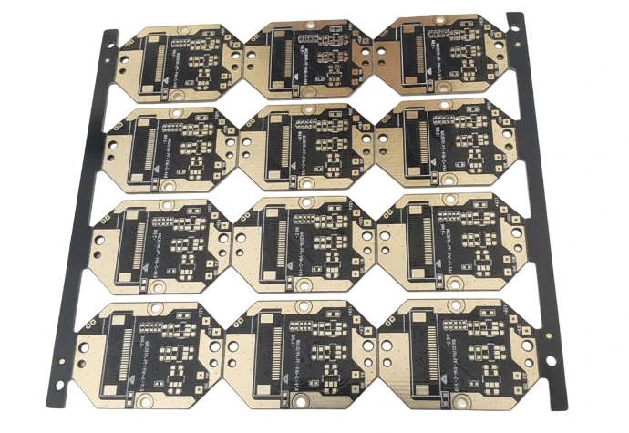
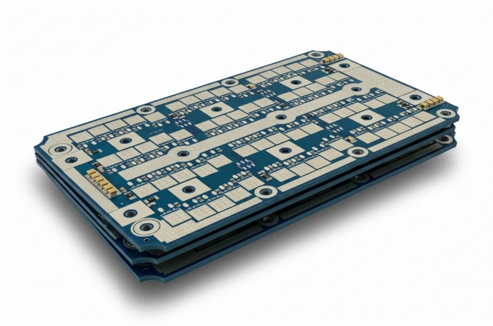
Thermal Stackup & CAM Engineering

CAM teams align copper thickness, dielectric conductivity, and machining tolerances to your thermal budget.

  • Confirm conductivity, thickness, and CTE for dielectrics and substrates.
  • Plan thermal via arrays, coin pockets, and alignment features.
  • Define vacuum lamination or bonding recipes.
  • Specify finishes compatible with LED reflectivity or power attachments.
  • Document Hi-Pot spacing, creepage, and clearance.
  • Provide handling instructions for bare metal bases and sharp edges.
  • Release packaging notes to prevent oxidation and scratching.

Manufacturing Execution & Feedback

Process engineers monitor lamination, plating, and test data and feed lessons back to design.

  • Monitor lamination/bonding pressure and record per lot.
  • Measure dielectric thickness and copper surface roughness.
  • Inspect via fill, coin bonding, and cavity machining.
  • Validate surface finish thickness and uniformity.
  • Run thermal and electrical tests; archive IR/D5470 data.
  • Package with corrosion protection and mechanical supports.
5–20 W/cm²

Power Density

Depending on platform

120–190 W/m·K

Ceramic Conductivity

AlN platforms

10 oz

Copper Thickness

For heavy copper builds

4 kV

Hi-Pot Testing

For isolation layers

Advantages of High-Thermal PCBs

Higher power density, longer lifetime, and simplified assemblies.

Power Density

MCPCB and heavy copper designs move heat directly into the baseplate.

Reliability

Low-CTE substrates and embedded vias prevent solder fatigue.

Platform Flexibility

Mix ceramic, MCPCB, and FR-4 layers in one assembly.

Thermal Validation

ASTM D5470 and IR data prove thermal paths.

System Cost Savings

Reduce external heatsinks and wiring complexity.

Quick Turn Readiness

Standardized platforms accelerate prototypes.

Why Choose APTPCB?

Integrated thermal paths replace bulky heatsinks and wiring harnesses, letting you shrink enclosures and boost reliability.

LEDEV powerIndustrial drivesTelecom PAAerospaceMedical
APTPCB production line
Thermal-Path PCB Fabrication & Assembly

High-Thermal PCB Applications

When heat limits performance, engineered PCBs take over.

LED lighting, EV traction, telecom power amplifiers, aerospace radar, and industrial drives all rely on robust thermal paths.

LED & Display

Backlighting, signage, and entertainment lighting.

LED engineSignageStage lightingDisplay backlightArchitectural

EV & Transportation

Traction inverters, chargers, and thermal plates.

InverterChargerBMSDC-DCBattery cooling

Industrial Power

Drives, UPS, and automation gear under continuous load.

Motor drivesUPSRoboticsFactory controlHVAC

Telecom & RF

Power amplifiers, RF combiners, and base stations.

PARRUCombinersBackhaulMicrowave

Aerospace & Defense

Radar T/R modules and avionics heat spreaders.

RadarAvionicsEWSatcomMissile

Medical & Life Sciences

Laser drivers, imaging probes, and therapy devices.

LaserImagingTreatmentsDiagnosticsWearables

Rigid-Flex Thermal

Folded thermal harnesses for compact modules.

Rigid-flexEdge computeIoT modulesWearables

Test & Measurement

Power load banks, IR calibrators, and inspection tools.

Load bankCalibrationInspectionLab

High-Thermal Design Challenges & Solutions

Managing heat flow, isolation, and mechanical stresses requires careful material and process choices.

Common Design Challenges

01

Heat Flux vs. Platform

Choosing the wrong substrate overshoots budget or underperforms thermally.

02

Isolation & Hi-Pot

Thin dielectrics must hold high voltage without breakdown.

03

CTE Mismatch

Different materials expand differently, stressing solder joints.

04

Surface Finish Impact

Finish choice affects emissivity and solder wetting for LEDs.

05

Assembly Logistics

Large metal-backed boards need fixturing and bake cycles.

06

Validation Data

Without IR or D5470 proof, end customers may delay approval.

Our Engineering Solutions

01

Platform Selection Workshops

We match heat flux to MCPCB, ceramic, or heavy copper builds with cost tradeoffs.

02

Isolation Planning

Dielectric thickness and creepage rules ensured for Hi-Pot to 4 kV.

03

CTE Balancing

Material stacks and bonding films tuned to minimize stress.

04

Finish Optimization

Recommend ENIG, silver, or bare copper based on assembly and optical needs.

05

Thermal Test Packages

ASTM D5470, IR, and FEA correlations bundled with each lot.

How to Control High-Thermal PCB Cost

Thermal performance scales with material and machining cost—reserve premium substrates for true hotspots. Standardizing panel sizes, drill sets, and finishes keeps quick-turn builds affordable. Provide heat maps, isolation targets, and assembly plans so we can recommend the lightest viable construction.

01 / 08

Hybrid Platforms

Combine MCPCB or ceramic only under heat sources; use FR-4 elsewhere.

02 / 08

Define Test Scope

Full D5470/IR for qualification, sampling for production runs.

03 / 08

Optimize Dielectric Thickness

Choose the thinnest layer that meets voltage/thermal needs.

04 / 08

Selective Finishes

Apply silver or ENEPIG only on LED/power pads.

05 / 08

Standardize Hardware

Use common screws/press-fit inserts to limit machining time.

06 / 08

Collaborative DFx

Joint reviews catch over-spec’d copper or finish requirements.

07 / 08

Shared Panel Tooling

Panelize multiple engines to reuse fixtures and reduce scrap.

08 / 08

Material Forecasts

Reserve AlN/Al₂O₃ lots ahead of time to avoid expediting fees.

Certifications & Standards

Quality, environmental, and industry credentials supporting reliable manufacturing.

Certification
ISO 9001:2015

Quality management across thermal PCB manufacturing.

Certification
ISO 14001:2015

Environmental controls for metal core processing and plating.

Certification
ISO 13485:2016

Traceability for medical and lighting applications.

Certification
IATF 16949

Automotive APQP/PPAP coverage for EV and power electronics.

Certification
AS9100

Aerospace process governance.

Certification
UL 94 V-0 / UL 796

Safety and flammability compliance for dielectric systems.

Certification
IPC-6012 / 6013

Performance standards for rigid and flex-rigid boards.

Certification
RoHS / REACH

Hazardous substance compliance.

Selecting a High-Thermal Manufacturing Partner

  • MCPCB, ceramic, and heavy copper capability in-house.
  • Vacuum lamination, bonding, and coin insertion expertise.
  • Thermal testing lab with D5470 and IR imaging.
  • Hi-Pot testing to 4 kV for isolation-critical builds.
  • Assembly fixtures and finishing for LEDs/power modules.
  • 24-hour DFx feedback across thermal, mechanical, and assembly teams.
Selecting a high-thermal manufacturing partner

Quality & Cost Console

Process & Reliability Controls + Economic Levers

Unified dashboard connecting HDI quality checkpoints with the economic levers that compress cost.

Process & Reliability

Pre-Lamination Controls

Stack-Up Validation

  • Panel utilization+5–8%
  • Stack-up simulation±2% thickness
  • VIPPO planningPer lot
  • Material bake110 °C vacuum

Pre-Lamination Strategy

• Rotate outlines, mirror flex tails

• Share coupons across programs

• Reclaim 5-8% panel area

Registration

Laser & Metrology

Registration

  • Laser drill accuracy±12 μm
  • Microvia aspect ratio≤ 1:1
  • Coverlay alignment±0.05 mm
  • AOI overlaySPC logged

Laser Metrology

• Online laser capture

• ±0.05 mm tolerance band

• Auto-logged to SPC

Testing

Electrical & Reliability

Testing

  • Impedance & TDR±5% tolerance
  • Insertion lossLow-loss verified
  • Skew testingDifferential pairs
  • Microvia reliability> 1000 cycles

Electrical Test

• TDR coupons per panel

• IPC-6013 Class 3

• Force-resistance drift logged

Integration

Assembly Interfaces

Integration

  • Cleanroom SMTCarrier + ESD
  • Moisture control≤ 0.1% RH
  • Selective materialsLCP / low Df only where needed
  • ECN governanceVersion-controlled

Assembly Controls

• Nitrogen reflow

• Inline plasma clean

• 48h logistics consolidation

Architecture

Stack-Up Economics

Architecture

  • Lamination cyclesOptimize 1+N+1/2+N+2
  • Hybrid materialsLow-loss where required
  • Copper weightsMix 0.5/1 oz strategically
  • BOM alignmentStandard cores first

Cost Strategy

• Balance cost vs performance

• Standardize on common cores

• Low-loss only on RF layers

Microvia Planning

Via Strategy

Microvia Planning

  • Staggered over stacked-18% cost
  • Backdrill sharingCommon depths
  • Buried via reuseAcross nets
  • Fill specificationOnly for VIPPO

Via Cost Savings

• Avoid stacked microvias

• Share backdrill tools

• Minimize fill costs

Utilization

Panel Efficiency

Utilization

  • Outline rotation+4–6% yield
  • Shared couponsMulti-program
  • Coupon placementEdge pooled
  • Tooling commonalityPanel families

Panel Optimization

• Rotate for nesting efficiency

• Share test coupons

• Standardize tooling

Execution

Supply Chain & Coating

Execution

  • Material poolingMonthly ladder
  • Dual-source PPAPPre-qualified
  • Selective finishENIG / OSP mix
  • Logistics lanes48 h consolidation

Supply Chain Levers

• Pool low-loss material

• Dual-source laminates

• Match finish to need

High-Thermal PCB Manufacturing — Upload Data for Thermal Review

IPC / ISO certified thermal lines
Thermal + electrical validation included
MCPCB / ceramic / heavy copper options
Reliability data packaged for audits

Send stackups, heat maps, and isolation targets—our team replies with DFx notes, validation scope, and lead time within one business day.

High-Thermal PCB FAQ

Key answers on materials, finishes, testing, and assembly readiness.