ROGERS / PTFE / LOW-LOSS

Microwave PCB Manufacturing — RF & Microwave Ready

Build RF/microwave PCBs on Rogers/PTFE laminates with tight impedance, cavity machining, and VNA testing for telecom, aerospace, and automotive applications.

  • RO4350B / RO4003C
  • RO3003 / RT/duroid
  • Hybrid FR-4
  • Cavity machining
  • ENEPIG / silver
  • VNA-tested

Get an Instant Quote

Full Quote →

Microwave PCB Fabrication & Assembly

APTPCB engineers design Rogers/PTFE stackups, dielectric thickness, and copper roughness aligned with RF performance targets.

We perform precision etching, cavity routing, plated slots, and via fences to maintain matching and Q factors.

Assembly covers silver/ENEPIG finishes, soldering, wire bonding, and coating for telecom, aerospace, and automotive RF modules.

Microwave PCB Fabrication & Assembly

Microwave Programs Delivered

RF boards for telecom, automotive radar, aerospace, and industrial sensing built on microwave-grade Rogers/PTFE laminates.

5G base stations

5G base stations

Aerospace radar

Aerospace radar

Automotive radar

Automotive radar

Industrial RF sensors

Industrial RF sensors

IoT & smart home

IoT & smart home

Medical RF devices

Medical RF devices

RF Performance Verified

Impedance coupons, VNA/S-parameters, and environmental tests ensure Microwave PCBs meet spec.

Download Capabilities
Rogers 4350B/4450RO3003/3035RT/duroidHybrid RF/FR-4±5% impedanceVNA testing

APTPCB Microwave Manufacturing Services

RF-focused fabrication with tight process control, finishing, and testing.

Microwave PCB Types

Backhaul radios, phased arrays, radar, mmWave, and hybrid RF/FR-4 systems.

  • Microstrip/stripline antennas
  • Hybrid RF/digital boards
  • Rigid-flex RF harnesses
  • Metal-backed RF structures
  • Multi-layer phased arrays

RF Via & Launch Structures

  • Via fences
  • Plated slots
  • Via-in-pad transitions
  • Backdrilled stubs
  • Embedded coins

Sample Microwave Stackups

  • RO4350B microstrip patch stackup
  • Hybrid RO3003 + FR-4 stripline
  • RT/duroid + copper coin radar module

Material & Design Guidelines

Select laminates with required Dk/Df, thickness, and copper roughness.

  • Define Dk/Df, dielectric thickness, and copper roughness.
  • Document finish (silver, ENEPIG) and bonding requirements.
  • Plan cavity depth and plating for filters.
  • Specify isolation for Hi-Pot and EMC.

Reliability & Validation

Microwave boards built on Rogers/PTFE laminates undergo VNA, impedance, humidity, and thermal cycling tests to meet telecom, automotive, and aerospace requirements.

Cost & Application Guidance

  • Use premium laminates only on RF layers; pair with FR-4 for logic.
  • Panelize antennas to maximize usage.
  • Select finishes based on assembly needs (silver vs ENEPIG).

Microwave PCB Manufacturing Flow

1

Stackup & RF Review

Align Dk/Df and copper roughness with frequency targets.

2

Imaging & Etch

LDI with compensation for RF geometries.

3

Cavity & Drill

Machine cavities, slots, and via fences.

4

Plating & Finish

Apply silver/ENEPIG with tight tolerances.

5

Assembly Prep

Plan soldering, wire bond, or coax attachment.

6

RF Validation

Impedance, VNA, and environmental testing.

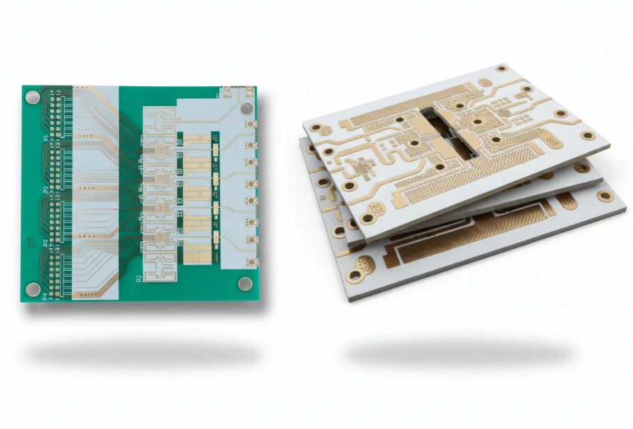
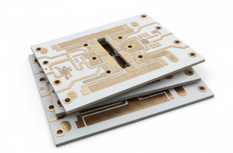
Microwave Stackup Engineering

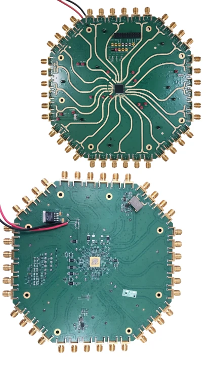
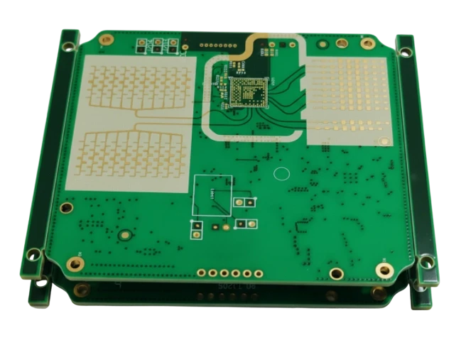
CAM + RF engineers guide stackups, cavity design, and impedance models.

  • Confirm laminates and acceptable alternates.
  • Define cavity routing and plating.
  • Plan impedance coupons and VNA fixtures.
  • Specify finishes and coating keep-outs.
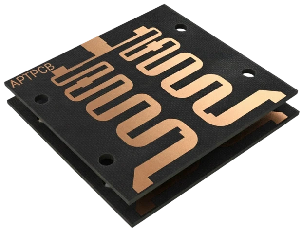
  • Document handling for PTFE/ceramic.

Manufacturing Execution

Process control for etch, plating, and testing ensures repeatability.

  • Monitor etch/dielectric thickness.
  • Inspect cavities, slots, and vias.
  • Validate finish thickness and adhesion.
  • Run impedance/VNA tests.
  • Package boards with protective films.
1–77 GHz

Frequency Range

Typical microwave builds

±5%

Impedance

Coupon verified

120 W/m·K

Thermal Options

Ceramic hybrids

4 kV

Hi-Pot

Isolation testing available

Advantages of Microwave PCBs

Low loss, stable Dk, and high reliability for RF designs.

Low Loss

Minimal insertion loss up to mmWave.

Stable Dk

Tight dielectric tolerance preserves matching.

Precision Machining

Cavities and slots produced accurately.

Hybrid Stackups

Combine microwave (Rogers/PTFE) signal layers with FR-4 for cost-efficient designs.

System Simplification

Integrate antennas and logic on one board.

Documentation

Complete SI packages.

Why Choose APTPCB?

Microwave laminates (Rogers/PTFE) deliver consistent RF performance across harsh environments.

TelecomAerospaceAutomotiveIndustrialMedicalConsumer
APTPCB production line

Microwave PCB Applications

5G/6G telecom, radar, satellite, automotive ADAS, medical, and industrial RF modules rely on microwave laminates built on Rogers/PTFE systems.

Low-loss stackups keep matching and gain stable.

Telecom & Wireless

RRU, BTS, and small cell radios.

RRUBTS

Automotive & ADAS

Radar, V2X, and telematics.

RadarV2X

Aerospace & Defense

Satcom, EW, and radar modules.

SatcomEW

Test & Measurement

RF instrumentation and calibration fixtures.

Instrumentation

Medical & Life Sciences

Imaging and therapy RF platforms.

ImagingTherapy

Industrial & IoT

Wireless sensors and gateways.

IoTSensors

Data Center & AI

Co-packaged optics and mmWave modules.

Co-packagedmmWave

Energy & Industrial

RF power amplifiers and sensors.

PASensors

Microwave Design Challenges & Solutions

Keep impedance, cavity, and finish control in check for RF fidelity.

Common Design Challenges

01

Material Availability

Premium laminates require lead time.

02

Cavity Machining

Tight tolerances needed for filters and waveguides.

03

Impedance Control

Any variation detunes matching networks.

04

Surface Finish

Finish affects solderability, bondability, and insertion loss.

05

Environmental Stability

Humidity and temperature can shift Dk.

06

Testing & Documentation

RF customers expect detailed VNA reports.

Our Engineering Solutions

01

Material Planning

Reserve microwave-grade Rogers laminates and define acceptable alternates.

02

Machining Playbooks

Set depth, plating, and tolerance standards.

03

Impedance Modeling

Stackup simulations plus coupon testing per lot.

04

Finish Guidance

Silver, ENIG, or ENEPIG recommendations.

05

Environmental Testing

Humidity and thermal cycling available.

How to Control Microwave PCB Cost

Microwave/Rogers PTFE materials are premium—reserve them for RF layers and pair with FR-4 elsewhere. Standardize stackups, finishes, and test scopes to keep lead time and pricing predictable. Tactics that keep microwave laminates and hybrid stack-ups under control.

01 / 08

Hybrid Stackups

Use microwave laminates only where needed.

02 / 08

Test Scope Planning

Define when full VNA testing is required.

03 / 08

DFx Collaboration

Early reviews prevent over-spec’d machining.

04 / 08

Panel Optimization

Panelize antennas for better yield.

05 / 08

Shared Fixtures

Reuse assembly fixtures across similar designs.

06 / 08

Finish Playbooks

Choose finishes based on true needs.

07 / 08

Finish Alignment

Silver vs ENEPIG vs ENIG based on application.

08 / 08

Material Forecasting

Reserve laminates for recurring builds.

Certifications & Standards

Quality, environmental, and industry credentials supporting reliable manufacturing.

Certification
ISO 9001:2015

Quality management for RF PCB fabrication.

Certification
ISO 14001:2015

Environmental controls for lamination and plating.

Certification
ISO 13485:2016

Traceability for medical RF builds.

Certification
IATF 16949

Automotive compliance for radar PCBs.

Certification
AS9100

Aerospace governance for satcom and avionics.

Certification
IPC-6012 Class 3

Performance standard for high-reliability RF PCBs.

Certification
UL 94 V-0 / UL 796

Flammability and dielectric compliance.

Certification
RoHS / REACH

Hazardous substance compliance.

Selecting a Microwave Manufacturing Partner

  • Microwave (Rogers/PTFE) material expertise.
  • RF machining (cavities, slots) in-house.
  • VNA/S-parameter testing.
  • Selective finishes and assembly support.
  • Environmental testing capability.
  • 24-hour RF DFx feedback.
Selecting a Microwave Manufacturing Partner

Quality & Cost Console

Process & Reliability Controls + Economic Levers

Unified dashboard connecting HDI quality checkpoints with the economic levers that compress cost.

Process & Reliability

Pre-Lamination Controls

Stack-Up Validation

  • Panel utilization+5–8%
  • Stack-up simulation±2% thickness
  • VIPPO planningPer lot
  • Material bake110 °C vacuum

Pre-Lamination Strategy

• Rotate outlines, mirror flex tails

• Share coupons across programs

• Reclaim 5-8% panel area

Registration

Laser & Metrology

Registration

  • Laser drill accuracy±12 μm
  • Microvia aspect ratio≤ 1:1
  • Coverlay alignment±0.05 mm
  • AOI overlaySPC logged

Laser Metrology

• Online laser capture

• ±0.05 mm tolerance band

• Auto-logged to SPC

Testing

Electrical & Reliability

Testing

  • Impedance & TDR±5% tolerance
  • Insertion lossLow-loss verified
  • Skew testingDifferential pairs
  • Microvia reliability> 1000 cycles

Electrical Test

• TDR coupons per panel

• IPC-6013 Class 3

• Force-resistance drift logged

Integration

Assembly Interfaces

Integration

  • Cleanroom SMTCarrier + ESD
  • Moisture control≤ 0.1% RH
  • Selective materialsLCP / low Df only where needed
  • ECN governanceVersion-controlled

Assembly Controls

• Nitrogen reflow

• Inline plasma clean

• 48h logistics consolidation

Architecture

Stack-Up Economics

Architecture

  • Lamination cyclesOptimize 1+N+1/2+N+2
  • Hybrid materialsLow-loss where required
  • Copper weightsMix 0.5/1 oz strategically
  • BOM alignmentStandard cores first

Cost Strategy

• Balance cost vs performance

• Standardize on common cores

• Low-loss only on RF layers

Microvia Planning

Via Strategy

Microvia Planning

  • Staggered over stacked-18% cost
  • Backdrill sharingCommon depths
  • Buried via reuseAcross nets
  • Fill specificationOnly for VIPPO

Via Cost Savings

• Avoid stacked microvias

• Share backdrill tools

• Minimize fill costs

Utilization

Panel Efficiency

Utilization

  • Outline rotation+4–6% yield
  • Shared couponsMulti-program
  • Coupon placementEdge pooled
  • Tooling commonalityPanel families

Panel Optimization

• Rotate for nesting efficiency

• Share test coupons

• Standardize tooling

Execution

Supply Chain & Coating

Execution

  • Material poolingMonthly ladder
  • Dual-source PPAPPre-qualified
  • Selective finishENIG / OSP mix
  • Logistics lanes48 h consolidation

Supply Chain Levers

• Pool low-loss material

• Dual-source laminates

• Match finish to need

Microwave PCB Manufacturing — Upload Data for RF Review

Talk to RF Engineers
IPC Class 3 RF lines
Low-loss expertise
Hybrid stackups
RF validation included

Share stackups, frequency targets, and assembly plans—we respond with DFx notes, SI plan, and timeline within one business day.

Microwave PCB FAQ

Questions on materials, finishes, and testing.