Detection of Hidden Defects
Uncovers critical issues including solder voids, misalignments, solder bridging, and internal cracks or breaks that would otherwise remain invisible until product failure.
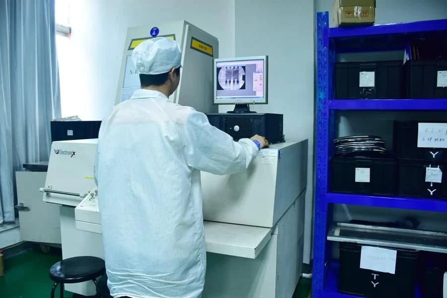
X-Ray & CT Inspection
For advanced, high-density electronics, many of the most critical defects are completely hidden—buried inside vias, sealed between layers, or located under BGA and bottom-terminated packages. APTPCB's PCB X-Ray Inspection Services provide a non-destructive way to 'see inside' your boards and assemblies, allowing you to verify build quality and identify hidden defects before products reach your customers.
A controlled beam of X-rays is directed at the PCB, penetrating through its various layers and components. Different materials absorb X-rays to varying degrees, which creates distinct contrast in the resulting image. A high-resolution detector on the opposite side of the PCB captures this image, providing a clear visualization of the board's internal structure.
Uncovers critical issues including solder voids, misalignments, solder bridging, and internal cracks or breaks that would otherwise remain invisible until product failure.
Provides reliable inspection of multi-layer boards, accurate assessment of dense designs, and assembly validation for miniaturized and hidden-joint components.
Catches latent defects early to prevent field failures, reduce warranty claims, and ensure safety and reliability of critical electronic systems.
Reduces rework and scrap rates, improves overall yield, and prevents problems from compounding into larger, more costly rectifications.
Contact APTPCB today to receive a quote or discuss how our X-ray inspection services can elevate your PCB quality assurance process.