ALN • AL₂O₃ • DBC/DPC

Ceramic PCB Manufacturing — Thermal & RF Performance

AlN, Al₂O₃, and DBC/DPC ceramic PCBs with 120–190 W/m·K conductivity, embedded copper, and Class 3 inspection for power, RF, and medical electronics.

  • AlN / Al₂O₃ / DBC
  • 120–190 W/m·K
  • Copper-filled vias
  • Wire bond ready
  • Hi-Pot 4 kV
  • Class 3 inspection

Get an Instant Quote

Full Quote →

Ceramic PCB Fabrication & Assembly

We engineer ceramic stackups (AlN, Al₂O₃, DBC/DPC) with thick copper, plated vias, and selective finishes to move heat efficiently and provide RF stability.

Our CAM team plans laser patterning, copper etch, via fill, and metallization to support wire bond, solder attach, and high-voltage isolation.

Assembly support includes silver sintering, solder attach, wire/ribbon bonding, and conformal coating tailored to ceramic substrates.

Ceramic PCB Fabrication & Assembly

Ceramic Programs Delivered

Power modules, RF amplifiers, medical devices, and aerospace electronics that leverage ceramic platforms.

Power modules

Power modules

LED/laser drivers

LED/laser drivers

Radar & RF modules

Radar & RF modules

Medical imaging

Medical imaging

Automotive power

Automotive power

Industrial sensing

Industrial sensing

Thermal & Electrical Reliability

ASTM D5470 conduction, Hi-Pot 4 kV, and wire bond validation ensure ceramic boards meet mission-critical requirements.

Download Capabilities
AlN / Al₂O₃DBC / DPC120–190 W/m·KWire bond readyHi-Pot 4 kVThermal vias

APTPCB Ceramic Manufacturing Services

We deliver DPC, DBC, and thick copper ceramic PCBs with turnkey assembly and testing.

Ceramic PCB Types

DPC AlN, DBC Al₂O₃, copper-backed ceramic, hybrid ceramic/FR-4, and microchannel designs.

  • DPC AlN microstrip
  • DBC Al₂O₃ power substrates
  • Ceramic + copper coin hybrids
  • Ceramic sensors with plated vias
  • Metal-backed ceramic

Thermal Vias & Coins

  • Copper-filled thermal vias
  • Embedded coins
  • Laser-drilled cavities
  • Plated slots for connectors
  • Wire bond pads

Sample Ceramic Structures

  • 0.63 mm AlN with 35 μm Cu
  • DBC 0.32 mm Al₂O₃ with 150 μm Cu
  • Hybrid ceramic + FR-4 stackup

Material & Design Guidelines

Match conductivity, dielectric strength, and CTE to device requirements.

  • Specify AlN/Al₂O₃ conductivity and thickness.
  • Define copper thickness for thermal and current targets.
  • Document isolation requirements for Hi-Pot tests.
  • Call out surface finish (silver, ENEPIG) for assembly.

Reliability & Validation

Ceramic boards undergo D5470 conduction, Hi-Pot, wire pull, shear, and thermal cycling with documented reports.

Cost & Application Guidance

  • Use premium AlN only where heat flux demands it.
  • Panelize small modules to maximize substrate usage.
  • Select finishes aligned with assembly (silver vs ENEPIG).

Ceramic PCB Manufacturing Flow

1

Stackup & Thermal Review

Align conductivity, thickness, and copper features.

2

Patterning & Metallization

Laser or photo imaging, copper deposition, and etch.

3

Via Drilling & Fill

Drill, plate, and fill thermal vias or coins.

4

Surface Finish & Mask

Apply silver, ENEPIG, or specialized finishes.

5

Assembly Preparation

Plan solder attach, wire bond, or sintering steps.

6

Validation & Test

D5470, Hi-Pot, wire pull, and inspection.

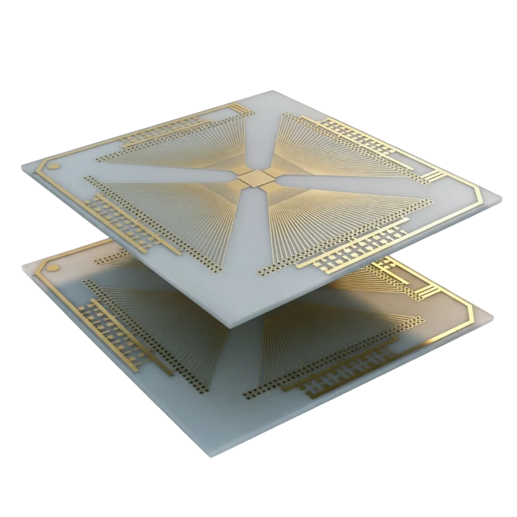
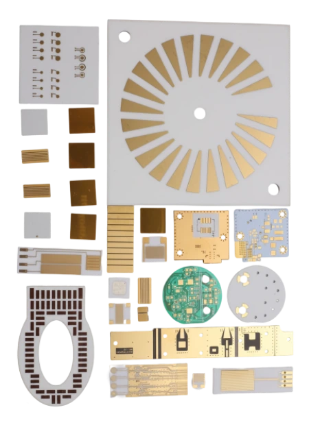
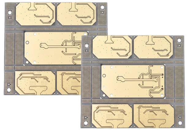
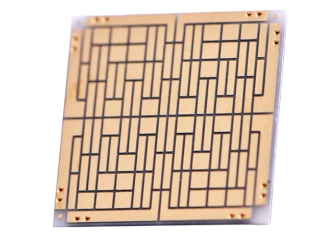
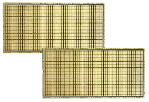
Ceramic Stackup Engineering

We plan dielectric, copper, and via features to meet thermal and electrical specs.

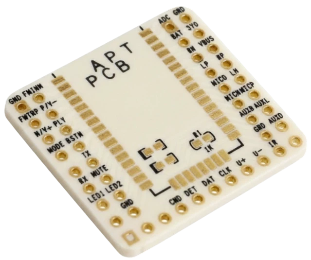
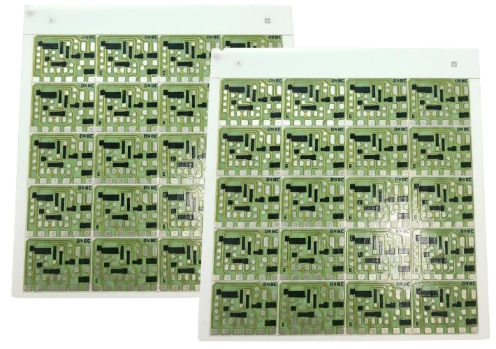
  • Confirm substrate type and conductivity.
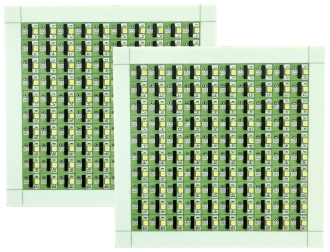
  • Define copper thickness and plating requirements.
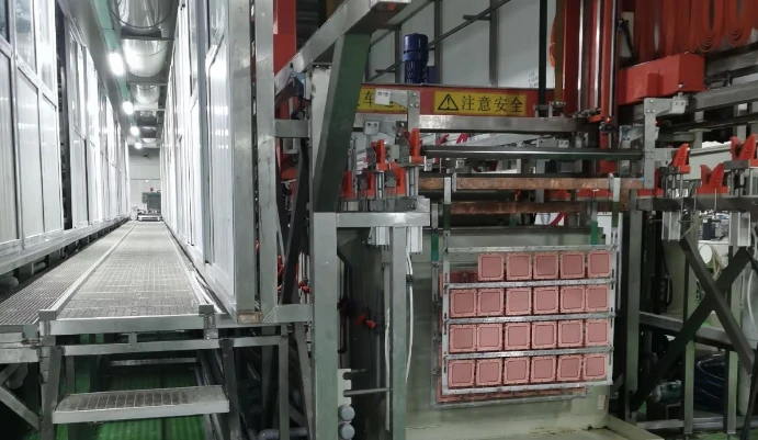
  • Plan laser drilling and cavity machining.
  • Specify finishes and masking.
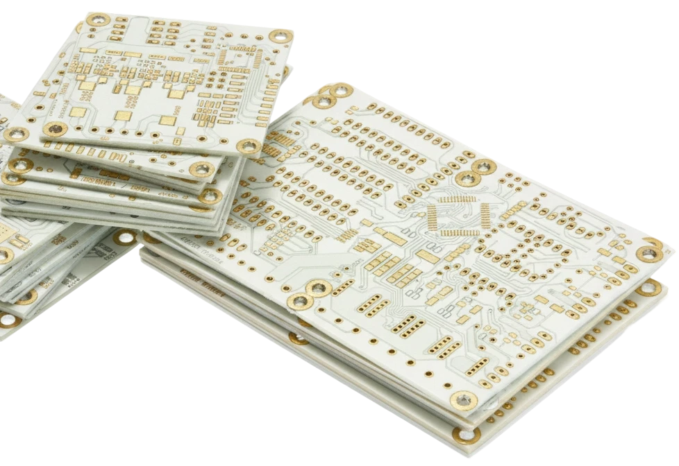
  • Document bake/handling for ceramic panels.
  • Provide packaging instructions for fragile substrates.

Manufacturing Execution

SPC on metallization, via fill, and testing ensures repeatability.

  • Monitor metallization thickness.
  • Inspect via fill and adhesion.
  • Validate finish thickness and wire bond readiness.
  • Perform Hi-Pot and thermal tests.
  • Package with foam and rigid trays to avoid damage.
120–190 W/m·K

Conductivity

AlN and Al₂O₃ options

4 kV

Hi-Pot

Isolation per lot

10–350 μm

Copper Thickness

DBC/DPC capability

Wire bond ready

Assembly

ENEPIG or silver finish

Advantages of Ceramic PCBs

High thermal conductivity, low CTE, and RF performance.

Thermal Performance

120–190 W/m·K conductivity removes heat efficiently.

Reliability

Low CTE prevents solder fatigue.

Integration

Copper coins, vias, and cavities built-in.

Wire Bond Ready

ENEPIG/Ag finishes for bond wires.

System Simplification

Eliminates extra heat spreaders.

Documentation

Thermal & electrical reports included.

High-Voltage Isolation

Hi-Pot screening up to 4 kV secures EV, medical, and industrial power modules.

Power Density Optimization

Thermal simulation support aligns via fields, coins, and die attach for compact layouts.

Why Choose APTPCB?

Ceramic substrates handle heat and RF demands better than standard FR-4.

Power modulesRFMedicalAerospaceLED/laserSensors
APTPCB production line
Ceramic plating

Ceramic PCB Applications

Power modules, RF/microwave, medical, aerospace, and automotive applications benefit from ceramic substrates.

High thermal conductivity and isolation keep performance stable.

Power Electronics

IGBT/SiC modules and converters.

IGBTSiCConverters

RF & Telecom

PA, T/R modules, and radar.

PARadarRF

Aerospace & Defense

Mission-critical electronics.

AvionicsDefense

Medical & Life Sciences

Imaging probes and therapy devices.

ImagingTherapy

Automotive & EV

Onboard chargers and lighting.

OBCLighting

Industrial & Sensors

High-temp sensors and inspection tools.

SensorsInspection

Rigid-Flex Hybrid

Ceramic with flex tails for compact modules.

Rigid-flexEdge devices

Test & Measurement

Load banks and metrology tools.

Load bankMetrology

Ceramic Design Challenges & Solutions

Manage thermal, mechanical, and assembly constraints unique to ceramic substrates.

Common Design Challenges

01

Material Availability

AlN lead times require early planning.

02

Surface Finish Choice

Finish impacts reflectivity, solderability, and bonding.

03

CTE Mismatch

Bonding dissimilar materials needs careful design.

04

Isolation vs. Conductivity

Balancing dielectric thickness and heat flow.

05

Fragility & Handling

Ceramic panels need custom fixturing and packaging.

06

Validation Documentation

Customers require detailed thermal/electrical reports.

Our Engineering Solutions

01

Material Planning

Reserve AlN/Al₂O₃ lots and define alternates.

02

Finish Playbook

Select silver/ENEPIG based on assembly needs.

03

CTE Matching

Design guidance for bonding to metal bases or FR-4.

04

Thermal Modeling

Simulate conduction paths before fab.

05

Packaging & Handling Kits

Custom trays and instructions ship with each lot.

How to Control Ceramic PCB Cost

Ceramic substrates and thick copper are expensive—reserve them for zones that truly need extreme thermal performance. Panelize small modules and reuse stackups to minimize waste and lead time. Provide heat flux, isolation, and assembly details early so we can choose the most cost-effective ceramic platform.

01 / 08

Targeted Platforms

Use AlN only for high flux; Al₂O₃ for moderate needs.

02 / 08

Test Scope Planning

Run full validation for qualification, sampling for volume.

03 / 08

DFx Collaboration

Early reviews prevent over-spec’d copper or finish.

04 / 08

Panel Optimization

Combine multiple small boards per panel.

05 / 08

Shared Fixtures

Reuse bonding and assembly fixtures across builds.

06 / 08

Hybrid Stackups

Combine ceramic under hotspots with FR-4 elsewhere.

07 / 08

Finish Alignment

Apply ENEPIG only on bond pads; use silver elsewhere.

08 / 08

Material Forecasting

Reserve ceramic substrates to avoid expedite fees.

Certifications & Standards

Quality, environmental, and industry credentials supporting reliable manufacturing.

Certification
ISO 9001:2015

Quality management for ceramic PCB fabrication.

Certification
ISO 14001:2015

Environmental controls for copper bonding and plating.

Certification
ISO 13485:2016

Traceability for medical ceramic modules.

Certification
IATF 16949

Automotive APQP/PPAP for Si₃N₄ AMB substrates.

Certification
AS9100

Aerospace build governance.

Certification
IPC-6012 / 6013

Rigid and rigid-flex performance classes.

Certification
UL 94 V-0 / UL 796

Dielectric safety and copper-clad compliance.

Certification
RoHS / REACH

Hazardous substance compliance.

Selecting a Ceramic Manufacturing Partner

  • DPC/DBC capability in-house.
  • Thermal and electrical validation labs.
  • Wire bond and solder attach support.
  • Hi-Pot testing up to 4 kV.
  • Automotive/aerospace documentation.
  • 24-hour DFx feedback.
Engineers reviewing ceramic PCBs

Quality & Cost Console

Process & Reliability Controls + Economic Levers

Unified dashboard connecting HDI quality checkpoints with the economic levers that compress cost.

Process & Reliability

Pre-Lamination Controls

Stack-Up Validation

  • Panel utilization+5–8%
  • Stack-up simulation±2% thickness
  • VIPPO planningPer lot
  • Material bake110 °C vacuum

Pre-Lamination Strategy

• Rotate outlines, mirror flex tails

• Share coupons across programs

• Reclaim 5-8% panel area

Registration

Laser & Metrology

Registration

  • Laser drill accuracy±12 μm
  • Microvia aspect ratio≤ 1:1
  • Coverlay alignment±0.05 mm
  • AOI overlaySPC logged

Laser Metrology

• Online laser capture

• ±0.05 mm tolerance band

• Auto-logged to SPC

Testing

Electrical & Reliability

Testing

  • Impedance & TDR±5% tolerance
  • Insertion lossLow-loss verified
  • Skew testingDifferential pairs
  • Microvia reliability> 1000 cycles

Electrical Test

• TDR coupons per panel

• IPC-6013 Class 3

• Force-resistance drift logged

Integration

Assembly Interfaces

Integration

  • Cleanroom SMTCarrier + ESD
  • Moisture control≤ 0.1% RH
  • Selective materialsLCP / low Df only where needed
  • ECN governanceVersion-controlled

Assembly Controls

• Nitrogen reflow

• Inline plasma clean

• 48h logistics consolidation

Architecture

Stack-Up Economics

Architecture

  • Lamination cyclesOptimize 1+N+1/2+N+2
  • Hybrid materialsLow-loss where required
  • Copper weightsMix 0.5/1 oz strategically
  • BOM alignmentStandard cores first

Cost Strategy

• Balance cost vs performance

• Standardize on common cores

• Low-loss only on RF layers

Microvia Planning

Via Strategy

Microvia Planning

  • Staggered over stacked-18% cost
  • Backdrill sharingCommon depths
  • Buried via reuseAcross nets
  • Fill specificationOnly for VIPPO

Via Cost Savings

• Avoid stacked microvias

• Share backdrill tools

• Minimize fill costs

Utilization

Panel Efficiency

Utilization

  • Outline rotation+4–6% yield
  • Shared couponsMulti-program
  • Coupon placementEdge pooled
  • Tooling commonalityPanel families

Panel Optimization

• Rotate for nesting efficiency

• Share test coupons

• Standardize tooling

Execution

Supply Chain & Coating

Execution

  • Material poolingMonthly ladder
  • Dual-source PPAPPre-qualified
  • Selective finishENIG / OSP mix
  • Logistics lanes48 h consolidation

Supply Chain Levers

• Pool low-loss material

• Dual-source laminates

• Match finish to need

Ceramic PCB Manufacturing — Upload Data for Thermal Review

IPC Class 3 ceramic lines
High conductivity platforms
DBC/DPC expertise
Full validation data

Share stackups, heat flux maps, and assembly requirements—we reply with DFx notes, cost, and timeline within one business day.

Ceramic PCB FAQ

Common questions about materials, conductivity, and assembly.