RF / MICROWAVE / 5G

Antenna PCB Manufacturing — Rogers & Hybrid RF Platforms

Design RF and microwave antenna PCBs on Rogers/PTFE, hybrid FR-4, or copper-backed structures with precise impedance, cavity machining, and VNA testing.

  • Rogers / PTFE
  • Hybrid RF/FR-4
  • Cavity machining
  • ENEPIG / silver
  • ±5% impedance
  • VNA / S-parameters

Get an Instant Quote

Full Quote →

Antenna PCB Fabrication & Assembly

APTPCB engineers model antenna stackups, dielectric constants, and ground references across Rogers, PTFE, and hybrid builds.

We control etch compensation, cavity routing, plated slots, and copper roughness so antennas maintain matching and gain.

Assembly services include selective silver/ENEPIG, press-fit coax, and conformal coating to protect RF structures.

Antenna PCB Fabrication & Assembly

Antenna Programs Delivered

5G/6G radios, radar, IoT, aerospace, and automotive antennas built on RF platforms.

5G massive MIMO arrays

5G massive MIMO arrays

Aerospace radar antennas

Aerospace radar antennas

Automotive V2X antennas

Automotive V2X antennas

IoT/smart home antennas

IoT/smart home antennas

Consumer wireless devices

Consumer wireless devices

Test & measurement antennas

Test & measurement antennas

RF Performance Validated

VNA S-parameters, impedance coupons, and IR thermography ensure antennas meet design specs.

Download Capabilities
Rogers / PTFEHybrid FR-4ENEPIG / silverCavity routing±5% impedanceVNA testing

APTPCB Antenna PCBs

RF-focused manufacturing with precise dielectric control and assembly support.

Antenna PCB Types

Patch, slot, phased array, mmWave, and conformal antennas.

  • Microstrip patch arrays
  • Stripline phased arrays
  • Hybrid RF + control boards
  • Conformal antennas
  • Active antenna modules

Via & Launch Structures

  • Plated via fences
  • Grounded coplanar waveguide vias
  • Via-in-pad transitions
  • Plated slots for coax feeds
  • Embedded copper coins

Sample RF Stackups

  • RO4350B microstrip patch stackup
  • Hybrid RO3003/FR-4 phased array
  • PTFE + aluminum-backed radar antenna

Material & Design Guidelines

Select laminates (RO4350B, RO3003, RT/duroid) and copper roughness levels for frequency targets.

  • Document Dk/Df, dielectric thickness, and copper roughness.
  • Plan cavity routing for waveguides and filters.
  • Specify finishes (silver, ENEPIG) based on bonding.
  • Define isolation distances for Hi-Pot and EMC.

Reliability & Validation

RF boards undergo impedance/VNA tests, thermal shock, humidity, and cross-sections to ensure consistency.

Cost & Application Guidance

  • Use premium PTFE only on RF layers.
  • Panelize small antennas for efficient builds.
  • Select finishes aligned with assembly (silver vs ENEPIG).

Antenna PCB Manufacturing Flow

1

Stackup & RF Review

Align dielectric constants and layout with performance goals.

2

Imaging & Etch

LDI with fine compensation for RF geometries.

3

Cavity & Drill

Machine cavities, slots, and vias.

4

Plating & Finish

Apply silver/ENEPIG with tight thickness control.

5

Assembly Prep

Plan soldering, coax attachment, and coating.

6

Validation & Test

VNA, impedance, and environmental tests.

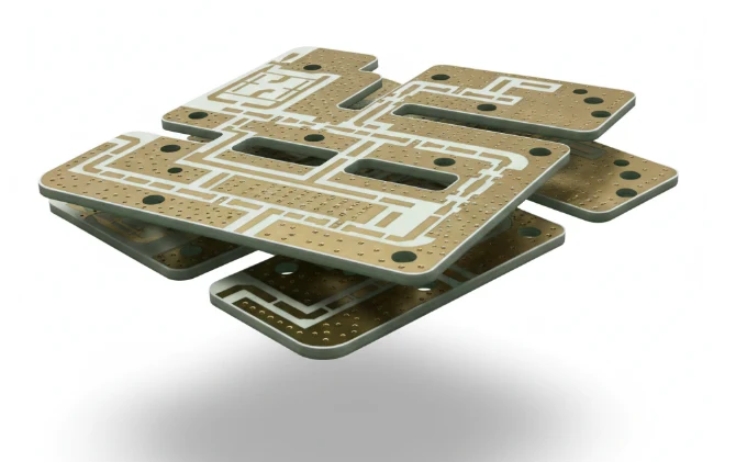
RF Stackup Engineering

We assist with stackup design, launch structures, and impedance modeling.

  • Confirm materials and acceptable alternates.
  • Define cavity depths and slot dimensions.
  • Plan impedance coupons and VNA fixtures.
  • Specify finishes and coating keep-outs.
  • Document handling for PTFE/ceramic substrates.

Manufacturing Execution

SPC monitors etch, plating, and testing for repeatability.

  • Monitor etch line width and copper thickness.
  • Inspect cavity depth and plated slots.
  • Validate finish thickness and adhesion.
  • Run impedance and VNA tests.
  • Package boards with surface protection.
1–40 GHz

Frequency Range

Typical antenna builds

±5%

Impedance

Coupon verified

120 W/m·K

Thermal Conductivity

Ceramic-backed options

4 kV

Hi-Pot

Isolation testing available

Advantages of APTPCB Antenna PCBs

Materials, machining, and testing tuned for RF performance.

RF Materials

Rogers/PTFE hybrids matched to frequency.

Precision Machining

Cavities, slots, and waveguides held tight.

Impedance Control

±5% validated with coupons.

Reliability

Environmental tests for telecom/aerospace.

Hybrid Stackups

Combine RF layers with FR-4 logic.

Documentation

Full SI data packages.

Antenna Tuning Support

Layout tweaks, cavity trims, and VNA sweeps keep gain and bandwidth on spec before mass build.

Environmental Endurance

Humidity, thermal cycling, and salt-mist screening make outdoor and telecom arrays mission ready.

Why Choose APTPCB?

We combine RF stackup expertise with advanced fabrication for consistent antennas.

TelecomAerospaceAutomotiveIoTMedicalIndustrial
APTPCB production line
production line

Antenna PCB Applications

5G/6G, radar, automotive V2X, IoT, aerospace, and medical antennas rely on precise RF stackups.

Stable materials and machining keep matching and gain on target.

Telecom & Wireless

Massive MIMO and base station arrays.

5GRRUBTS

Automotive & V2X

ADAS radar, telematics, and V2X antennas.

ADASV2X

Aerospace & Defense

Radar, EW, and satellite antennas.

RadarEWSatcom

Test & Measurement

Calibration and instrumentation antennas.

CalibrationInstrumentation

Medical & Life Sciences

Diagnostic and therapy RF devices.

ImagingTherapy

IoT & Consumer

Smart home and wearable antennas.

Smart homeWearables

Industrial & Energy

Wireless sensors and inspection tools.

SensorsInspection

Data Center & AI

Co-packaged optics and mmWave modules.

Co-packaged opticsmmWave

Antenna Design Challenges & Solutions

Material, impedance, and cavity control are critical for antenna performance.

Common Design Challenges

01

Material Selection

Choosing the right Dk/Df combination for frequency.

02

Cavity Machining

Precise routing needed for waveguides and filters.

03

Impedance Control

Any variation detunes matching networks.

04

Surface Finish

Finish affects solderability, reflectivity, and bonding.

05

Environmental Stability

Moisture or temperature shifts can drift performance.

06

Documentation

Customers expect SI and test records.

Our Engineering Solutions

01

Material Playbooks

Recommend RF laminates and acceptable alternates.

02

Machining Guides

Cavity, slot, and plating tolerances defined upfront.

03

Impedance Modeling

Stackup simulations and coupon testing provided.

04

Finish Recommendations

Guidance on silver, ENEPIG, or bare copper.

05

Environmental Testing

Humidity and thermal cycling available.

How to Control Antenna PCB Cost

Use premium RF materials only where necessary; combine with FR-4 for control logic. Standardize cavity depths, finishes, and panel sizes to streamline quoting. Share frequency targets, antenna size, and assembly plans so we can build the most efficient platform.

01 / 08

Hybrid Stackups

Use PTFE only under RF sections.

02 / 08

Test Scope

Full VNA for qualification, sampling for production.

03 / 08

DFx Collaboration

Early reviews prevent over-spec’d machining.

04 / 08

Panel Planning

Panelize multiple antennas to maximize usage.

05 / 08

Shared Fixtures

Reuse assembly fixtures across SKUs.

06 / 08

Finish Playbooks

Standardize finish choices to cut cost.

07 / 08

Finish Alignment

Silver for RF, ENIG/OSP for control areas.

08 / 08

Material Forecasting

Reserve RF laminates for ongoing programs.

Certifications & Standards

Quality, environmental, and industry credentials supporting reliable manufacturing.

Certification
ISO 9001:2015

Quality management for fabrication, assembly, and testing.

Certification
ISO 14001:2015

Environmental controls across plating, lamination, and finishing.

Certification
ISO 13485

Medical device traceability, cleanliness, and documentation.

Certification
IATF 16949

Automotive APQP/PPAP with lot-level traceability.

Certification
AS9100

Aerospace-grade configuration and production controls.

Certification
IPC-6012 / 6013

Printed board reliability standards for rigid and flex builds.

Certification
UL 796 / UL 61010

Safety certifications covering flammability and insulation.

Certification
RoHS / REACH

Hazardous substance compliance with lot-backed declarations.

Selecting an Antenna Manufacturing Partner

  • RF materials and cavity machining in-house.
  • VNA/S-parameter test lab.
  • Selective finishes and coating support.
  • Environmental testing capability.
  • DFx feedback with RF engineers.
  • Traceable documentation for telecom/aerospace.
Selecting an Antenna Manufacturing Partner

Quality & Cost Console

Process & Reliability Controls + Economic Levers

Unified dashboard connecting HDI quality checkpoints with the economic levers that compress cost.

Process & Reliability

Pre-Lamination Controls

Stack-Up Validation

  • Panel utilization+5–8%
  • Stack-up simulation±2% thickness
  • VIPPO planningPer lot
  • Material bake110 °C vacuum

Pre-Lamination Strategy

• Rotate outlines, mirror flex tails

• Share coupons across programs

• Reclaim 5-8% panel area

Registration

Laser & Metrology

Registration

  • Laser drill accuracy±12 μm
  • Microvia aspect ratio≤ 1:1
  • Coverlay alignment±0.05 mm
  • AOI overlaySPC logged

Laser Metrology

• Online laser capture

• ±0.05 mm tolerance band

• Auto-logged to SPC

Testing

Electrical & Reliability

Testing

  • Impedance & TDR±5% tolerance
  • Insertion lossLow-loss verified
  • Skew testingDifferential pairs
  • Microvia reliability> 1000 cycles

Electrical Test

• TDR coupons per panel

• IPC-6013 Class 3

• Force-resistance drift logged

Integration

Assembly Interfaces

Integration

  • Cleanroom SMTCarrier + ESD
  • Moisture control≤ 0.1% RH
  • Selective materialsLCP / low Df only where needed
  • ECN governanceVersion-controlled

Assembly Controls

• Nitrogen reflow

• Inline plasma clean

• 48h logistics consolidation

Architecture

Stack-Up Economics

Architecture

  • Lamination cyclesOptimize 1+N+1/2+N+2
  • Hybrid materialsLow-loss where required
  • Copper weightsMix 0.5/1 oz strategically
  • BOM alignmentStandard cores first

Cost Strategy

• Balance cost vs performance

• Standardize on common cores

• Low-loss only on RF layers

Microvia Planning

Via Strategy

Microvia Planning

  • Staggered over stacked-18% cost
  • Backdrill sharingCommon depths
  • Buried via reuseAcross nets
  • Fill specificationOnly for VIPPO

Via Cost Savings

• Avoid stacked microvias

• Share backdrill tools

• Minimize fill costs

Utilization

Panel Efficiency

Utilization

  • Outline rotation+4–6% yield
  • Shared couponsMulti-program
  • Coupon placementEdge pooled
  • Tooling commonalityPanel families

Panel Optimization

• Rotate for nesting efficiency

• Share test coupons

• Standardize tooling

Execution

Supply Chain & Coating

Execution

  • Material poolingMonthly ladder
  • Dual-source PPAPPre-qualified
  • Selective finishENIG / OSP mix
  • Logistics lanes48 h consolidation

Supply Chain Levers

• Pool low-loss material

• Dual-source laminates

• Match finish to need

Antenna PCB Manufacturing — Upload Data for RF Review

Talk to RF Engineers
IPC Class 3 RF lines
Rogers/PTFE expertise
Hybrid stackups
RF validation included

Send stackups, frequency targets, and panel drawings—our team replies with DFx notes, SI plan, and lead time within one business day.

Antenna PCB FAQ

Answers on materials, finishes, and RF testing.