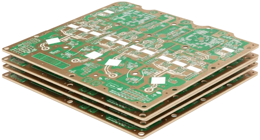
Multilayer PCB cross-section

4–32 LAYER BUILDS

Multilayer PCB Manufacturing — Dense HDI & High-Layer Backplanes

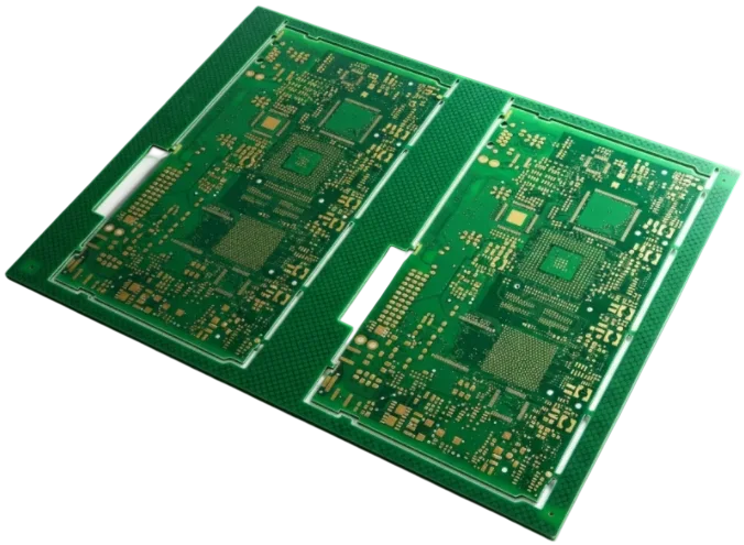
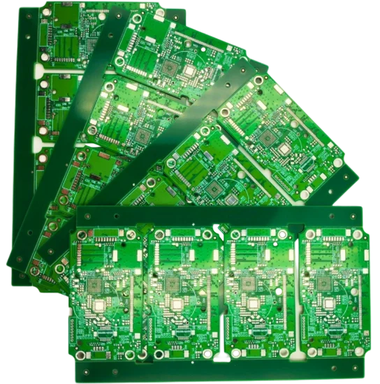
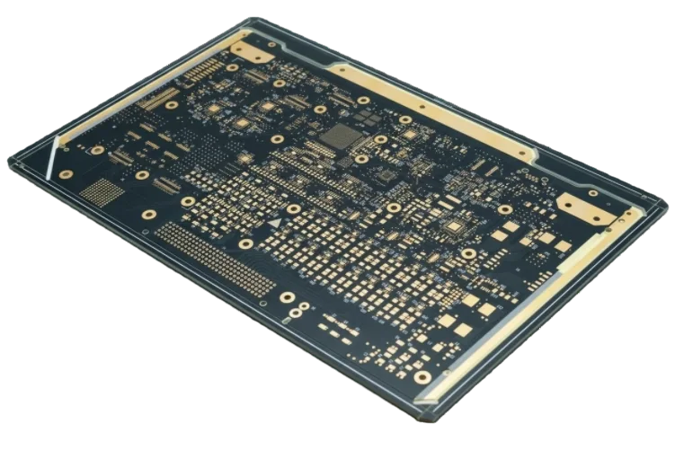
A multilayer PCB is a rigid board with multiple copper layers bonded through cores and prepregs; this service controls stack-up, sequential lamination, via architecture, and ±5% impedance across verified 4–32 layer builds.

  • 4–32 layer capability
  • Sequential lamination
  • HDI microvias
  • ±5% impedance
  • Backplane panel sizes
  • Class 3 inspection

Get an Instant Quote

Full Quote →
4–32 LayersLayer Count
3/3 mil + 0.05 mmFine Features
0.5–5 oz | 0.2–6.0 mmCopper & Thickness
3/3 mil minLine/Space
0.20 mm mech / 0.067 mm laserDrill
0.2–6.0 mmBoard Thickness
4–32Layer Capacity
1100×500 mmMax Panel
±5%Impedance
4–32 LayersLayer Count
3/3 mil + 0.05 mmFine Features
0.5–5 oz | 0.2–6.0 mmCopper & Thickness
3/3 mil minLine/Space
0.20 mm mech / 0.067 mm laserDrill
0.2–6.0 mmBoard Thickness
4–32Layer Capacity
1100×500 mmMax Panel
±5%Impedance

Multilayer PCB Fabrication & Assembly

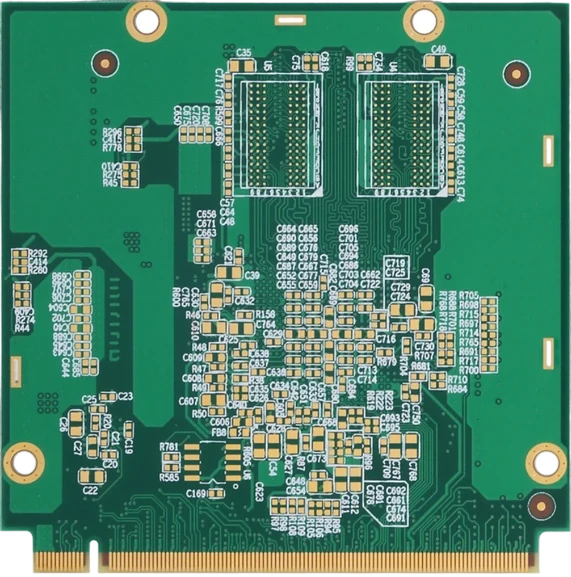
APTPCB manufactures multilayer PCBs from 4 layers through high layer counts to support complex routing density, multiple power domains, and tighter EMC demands. Our multilayer process covers sequential lamination, impedance-managed planes, mixed copper weights, and accurate layer registration—so electrical performance and mechanical stability remain consistent from prototype runs to volume builds.

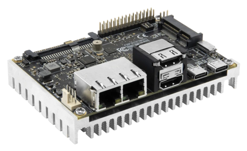
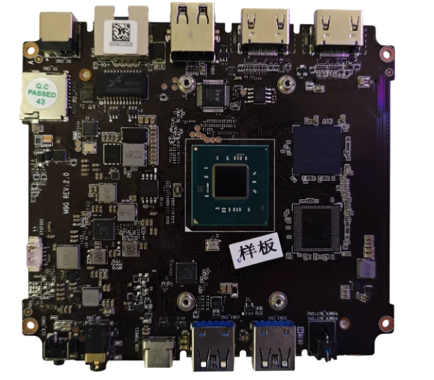
For multilayer PCB assembly, we manage dense and complex PCBA programs including large BGAs, mixed SMT/THT processes, and multi-stage testing requirements. With coordinated inspection and test planning, we help balance yield, reliability, and scalability—delivering multilayer assemblies that are production-ready, not just “sample-ready.”

Multilayer PCB fab

Multilayer Projects Delivered

Telecom backplanes, data-center fabrics, industrial controllers, and aerospace avionics built on multilayer stackups.

Data center fabrics

Data center fabrics

Telecom switches

Telecom switches

Aerospace avionics

Aerospace avionics

Industrial drives

Industrial drives

Automotive controllers

Automotive controllers

Compute modules

Compute modules

High-Layer Reliability

Impedance coupons, AOI/X-ray, CAF testing, and thermal stress verify multilayer builds that serve mission-critical markets.

Download Capabilities
4–32 layersHDI microviasBackplanes±5% impedanceCopper balancingLarge panels

APTPCB Multilayer Manufacturing Services

We engineer complex stackups with HDI, buried vias, and large format panels needed for telecom and industrial applications.

Multilayer Configurations

Standard multilayer, high-Tg, low-loss, HDI, rigid-flex, and backplane architectures.

  • Standard Multilayer – 6–16 layers for control electronics.
  • High-Layer Backplane – 24–32 layers with dual stripline groups.
  • HDI Multilayer – 1+N+1 or 2+N+2 microvia structures.
  • Low-Loss Multilayer – EM-370/I-Speed for 25–56 Gbps fabrics.
  • Rigid-Flex Multilayer – FR-4 cores tied to polyimide flex.

Via & Interconnect Options

  • Laser microvias
  • Buried vias
  • Stacked/staggered microvias
  • Backdrilled vias
  • Resin-filled via-in-pad

Sample Multilayer Stackups

  • 14-layer dual stripline backplane
  • 18-layer 2+N+2 HDI stackup
  • 24-layer low-loss telecom fabric

Material & Design Guidelines

Select laminates for Tg, Df, and CTE, plus copper weights per power layer.

  • Document Tg/Df, resin content, and copper distribution per layer.
  • Balance stackups to control bow/twist.
  • Call out prepreg styles compatible with sequential lamination.
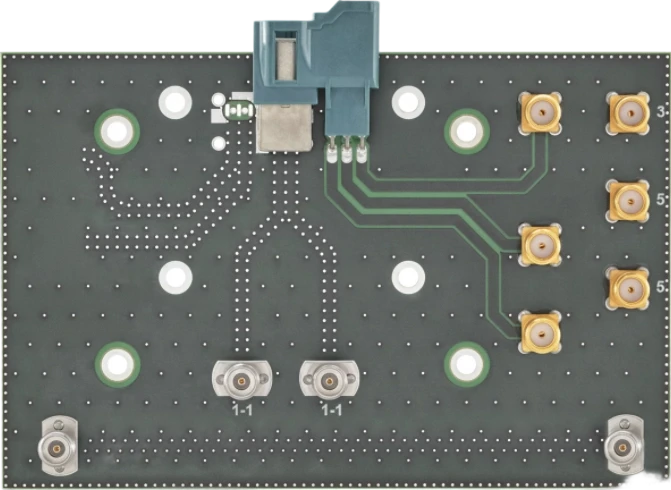
  • Provide impedance targets and tolerances for each routing layer.

Reliability & Validation

We run impedance coupons, X-ray, cross-sections, CAF, and thermal shock to ensure multilayer boards meet Class 3 and telecom/aerospace specs.

Cost & Application Guidance

  • Reuse proven stackups across product families.
  • Panelize large boards to maximize utilization.
  • Group drill sizes/backdrill depths to cut tooling cost.

Multilayer PCB Manufacturing Flow

1

Stackup & DFx Review

Align materials, lamination cycles, and impedance goals.

2

Core Prep & Imaging

LDI imaging for fine geometries.

3

Sequential Lamination

Controlled cycles for HDI and high-layer builds.

4

Drill, Fill & Backdrill

Precision drilling plus via fill/backdrill operations.

5

Surface Finish & Mask

Apply ENIG/ENEPIG/OSP with color options.

6

Testing & Inspection

Impedance, electrical, AOI, X-ray, and reliability tests.

Stackup & CAM

We simulate impedance, copper balance, and lamination sequences before release.

  • Confirm materials and acceptable alternates.
  • Define sequential lamination plan.
  • Plan impedance coupons and reference planes.
  • Specify via structures, fill, and backdrill requirements.
  • Document finish, coating, and baking instructions.
Manufacturing Execution

SPC-monitored lamination, drilling, plating, and inspection feed back to design.

  • Monitor lamination temperature/pressure.
  • Inspect drill quality and via fill.
  • Measure impedance coupons and archive data.
  • Perform AOI, X-ray, and cross-sections.
  • Package large panels with supports to avoid warpage.

Advantages of Multilayer PCBs

High density, high reliability, and scalable production.

High Density Routing

Support fine-pitch BGAs and SERDES fabrics.

Impedance Control

±5% tolerance for differential pairs.

Reliability

Class 3 inspection for harsh environments.

High-Speed Ready

Low-loss options for 25–56 Gbps.

Scalable

Prototype to mass production under one roof.

Documentation

Complete stackup + test reports.

Why Choose APTPCB?

Multilayer stackups integrate signal, power, and reference planes in one controlled platform.

APTPCB production line
Multilayer lamination • Microvia drilling • Backdrill

Multilayer PCB Applications

Telecom, datacenter, aerospace, automotive, medical, and industrial automation rely on multilayer stackups for density and reliability.

Balanced stackups combine signal, reference, and power planes in a single assembly.

Telecom & Network

Baseband, switch, and router fabrics.

SwitchRouterBaseband

Data Center & AI

Server backplanes and accelerator boards.

BackplaneAI

Automotive & EV

Central controllers and ADAS compute.

ADASCentral compute

Aerospace & Defense

Mission computers and avionics.

AvionicsMission computer

Industrial Automation

Robotics and motor drives.

RoboticsDrives

Medical & Imaging

Diagnostic instruments and imaging systems.

ImagingDiagnostics

Rigid-Flex Systems

Compact electronics needing mixed rigid/flex sections.

Rigid-flexWearables

Test & Measurement

ATE load boards and instrumentation.

ATEInstrumentation

Multilayer Design Challenges & Solutions

Control stackups, warpage, impedance, and sequential lamination without compromising yield.

Common Design Challenges

01

Stackup Complexity

High layer counts require balanced copper and dielectric selection.

02

Impedance & SI

Multiple routing layers need consistent dielectric control.

03

Warpage

Unbalanced copper or resin flow causes bow/twist on large panels.

04

Via Reliability

Deep vias and stacked microvias need proper plating and fill.

05

Backdrill Planning

Incorrect stub removal impacts signal integrity.

06

Documentation Load

Customers expect full stackup and test records.

Our Engineering Solutions

01

Stackup Modeling

We optimize dielectric selections, copper balance, and lamination sequences.

02

Impedance Simulation

Coupons and modeling keep SI targets within ±5%.

03

Warpage Control

Copper thieving, cross-hatching, and panel design prevent bow/twist.

04

Via Process Control

Via fill and plating plans maintain reliability.

05

Backdrill Tooling

Depth tables and verification ensure consistent stub removal.

How to Control Multilayer PCB Cost

Higher layer counts and HDI features add cost—apply them only where density demands. Standardize stackups, drill sets, and panel sizes to shorten quoting and fabrication. Share routing density, impedance, and panelization goals early so we can recommend the leanest build.

01 / 08

Stackup Reuse

Reuse qualified stackups for related products.

02 / 08

Finish Planning

Reserve ENEPIG for mixed assembly; use ENIG/OSP elsewhere.

03 / 08

DFx Collaboration

Early review catches over-constrained design rules.

04 / 08

Panel Optimization

Rotate and gang boards to improve yield.

05 / 08

Testing Scope

Define reliability testing frequency to avoid unnecessary costs.

06 / 08

Shared Tooling

Use common drill/lamination tooling to reduce NRE.

07 / 08

Depth Grouping

Group backdrill depths to minimize machine time.

08 / 08

Material Forecasting

Reserve low-loss materials for long programs.

Certifications & Standards

Quality, environmental, and industry credentials supporting reliable manufacturing.

Certification
ISO 9001:2015

Quality management for multilayer fabrication.

Certification
ISO 14001:2015

Environmental controls for press, plating, and imaging.

Certification
ISO 13485:2016

Traceability for medical and instrumentation builds.

Certification
IATF 16949

Automotive APQP/PPAP for high-layer control modules.

Certification
AS9100

Aerospace governance across sequential lamination.

Certification
IPC-6012 / 6013

Performance classes for rigid and rigid-flex stackups.

Certification
UL 94 V-0 / UL 796

Safety compliance for flame and dielectric metrics.

Certification
RoHS / REACH

Hazardous substance compliance.

Multilayer RFQ and Release Checklist

  • Gerber or ODB++, NC drill files, fabrication drawing, and controlled revision.
  • Layer order, finished thickness, copper weights, dielectric targets, and stack-up notes.
  • Approved laminate or performance targets for Tg, Dk, Df, thickness, and availability.
  • Controlled-impedance net classes, target values, tolerance, and coupon requirements.
  • Finished-hole table, microvia and via-fill notes, plus backdrill layers and residual-stub targets.
  • Board outline and panel constraints, surface finish, quantities, lead time, inspection class, and release documents.
Engineers reviewing multilayer stackups

Multilayer PCB Quality & Cost Console

Multilayer PCB Process & Economic Controls

Quality gates synced with the cost levers for complex control and compute systems.

Engineering Release

Stack-Up Release

Gate 01

  • Layer range4–32 layers
  • Stack-up revisionCustomer approved
  • Material systemReleased by part number
  • Impedance tableTargets attached

Release evidence

• Freeze layer order, finished thickness, copper weights, and dielectric targets.

• Resolve material substitutions before tooling or impedance modelling starts.

• Record the approved fabrication drawing and stack-up revision in the job package.

Inner Layers

Inner-Layer AOI Release

Gate 02

  • ImagingLDI
  • Trace / space3/3 mil minimum
  • AOI dispositionEach inner layer
  • Copper balanceReviewed before press

Release evidence

• Compare AOI findings with the released CAM data before lamination.

• Confirm tooling targets and copper distribution for the approved panel.

• Hold affected inner layers until opens, shorts, or registration findings are dispositioned.

Press Cycle

Lamination & Registration Release

Gate 03

  • Press recipeLogged by cycle
  • Sequential buildCycle order verified
  • Layer registrationX-ray targets checked
  • Bow / twist≤0.7%

Release evidence

• Record temperature, pressure, and dwell for each lamination cycle.

• Check registration targets before the build advances to drilling.

• Verify board construction and warpage against the released drawing.

Interconnect

Drill & Plating Release

Gate 04

  • Mechanical drill0.20 mm minimum
  • Laser microvia0.067 mm
  • BackdrillDepth plan verified
  • Plating evidenceMicrosection as required

Release evidence

• Match NC drill, finished-hole, via-fill, and backdrill notes to the released data.

• Verify registration and residual-stub requirements before final depth release.

• Retain plating and microsection records required by the inspection plan.

Electrical Test

Impedance & Electrical Release

Gate 05

  • Impedance tolerance±5%
  • Coupon correlationTDR recorded
  • Continuity / isolation100% electrical test
  • ExceptionsDisposition before release

Release evidence

• Correlate the released impedance table with the coupon and measured TDR result.

• Complete flying-probe or fixture testing according to lot and volume requirements.

• Close electrical exceptions before final inspection.

Shipment Release

Final Inspection & Documentation Release

Gate 06

  • DimensionsDrawing verified
  • Surface finishVisual acceptance
  • Lot traceabilityMaterial and process logs
  • Release packageCOC and test records

Release evidence

• Confirm dimensions, board thickness, bow/twist, marking, and finish against the drawing.

• Attach the specified AOI, electrical, impedance, and inspection records.

• Release the lot only against the approved revision and documentation list.

Architecture

Stack-Up Economics

Architecture

  • Lamination cyclesOptimize 1+N+1/2+N+2
  • Material mixHybrid when needed
  • Copper weights0.5/1 oz mix
  • BOM alignmentPreferred cores

Stack-Up Strategy

• Pick stack-ups that balance sequential lamination and via stacks demands.

• Standardize dielectric & copper sets per platform family.

• Apply premium laminates only where performance dictates.

Interconnect

Routing & Via Strategy

Interconnect

  • Via strategyStaggered priority
  • Backdrill planShared depths
  • Buried reuseMulti-net
  • VIP / tent usageAs required

Interconnect Controls

• Favor staggered/buried vias to avoid unnecessary fill cycles.

• Share drill maps, backdrills, and routing templates across builds.

• Limit via-in-pad or resin fill to fine-pitch or RF zones.

Utilization

Panel Efficiency

Utilization

  • Outline rotation+4–6% yield
  • Coupon sharingMulti-program
  • Tooling reusePanel families
  • Depanel strategyStandard tabs

Panel Optimization

• Rotate outlines and gang coupons to reclaim panel area.

• Re-use depanel tabs, fiducials, and tooling per family.

• Coordinate coupon placement for faster AOI and test.

Execution

Supply Chain & Finish

Execution

  • Material poolingMonthly ladder
  • Dual-sourcePPAP ready
  • Finish mixENIG / OSP
  • Logistics lanes48 h consolidation

Supply Levers

• Pool laminates, copper, and specialty films on a monthly cadence.

• Maintain dual-source approvals for critical materials.

• Align logistics lanes and 48 h consolidation windows per region.

Multilayer PCB FAQ

Answers on layer counts, materials, and testing.

Multilayer PCB Manufacturing — Upload Data for DFx Review

IPC Class 3 multilayer lines
4–32 layer capability
HDI & low-loss expertise
Reliability documentation

Send stackups, panel drawings, and impedance goals—we reply with DFx notes, cost, and timeline within one business day.