PCBA quality & acceptance

One inspection chain.Defined at each gate.

Connect material checks, process inspection and electrical evidence to product-specific acceptance and final release.
Quality route
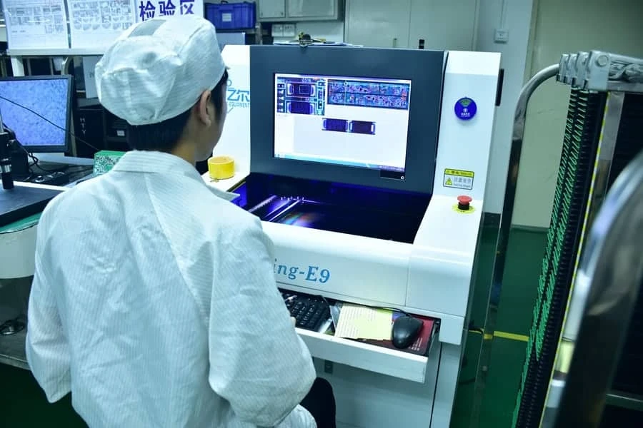
Operator reviewing a circuit board at an optical inspection station
Optical inspection contributes visible-feature evidence within the wider PCBA quality plan.

01 / Product-specific acceptance

Build an inspection chain around the actual product.

Every gate needs a purpose, a defined acceptance basis and a connection to the production lot.

Operator attending surface-mount assembly equipment and component feeders
Our PCBA quality inspection process is a multi-layered, systematic approach designed to detect and prevent defects from the very beginning. The goal: every PCBA you receive is “plug-and-play” ready for your product line without further intervention.

02 / Before production

Make manufacturing and test access part of design review.

Quality starts in the design phase. If you want to reduce defects and test difficulties from the start, we can assist before production begins:
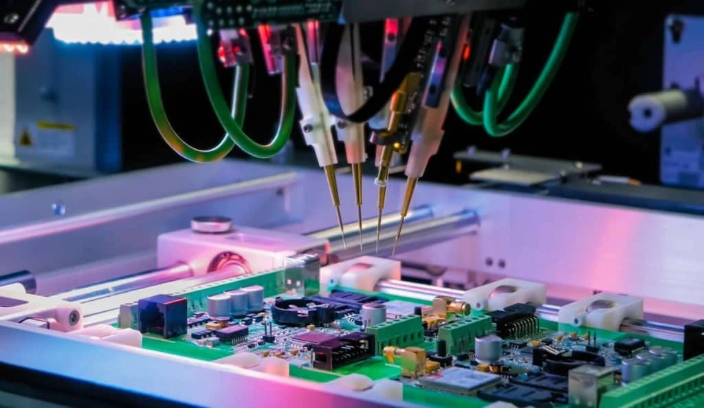
Movable electrical test probes positioned above a populated circuit board
Probe reach and the approved electrical program determine achievable coverage.

DFM (Design for Manufacturability) Review

We ensure your PCB designs are optimized for manufacturing efficiency.

DFT (Design for Testability) Support

We ensure your designs are structured to be easily tested during production, minimizing testing challenges later on.

PCB Layering, Routing, and Test Point Layout Suggestions

Our engineers work with your team to identify potential risks and address them early in the design phase, ensuring smoother production later on.

03 / Incoming material

Confirm the inputs before they reach placement.

All components, whether PCBs or electronic components, undergo rigorous inspection before they are even placed on the production line:
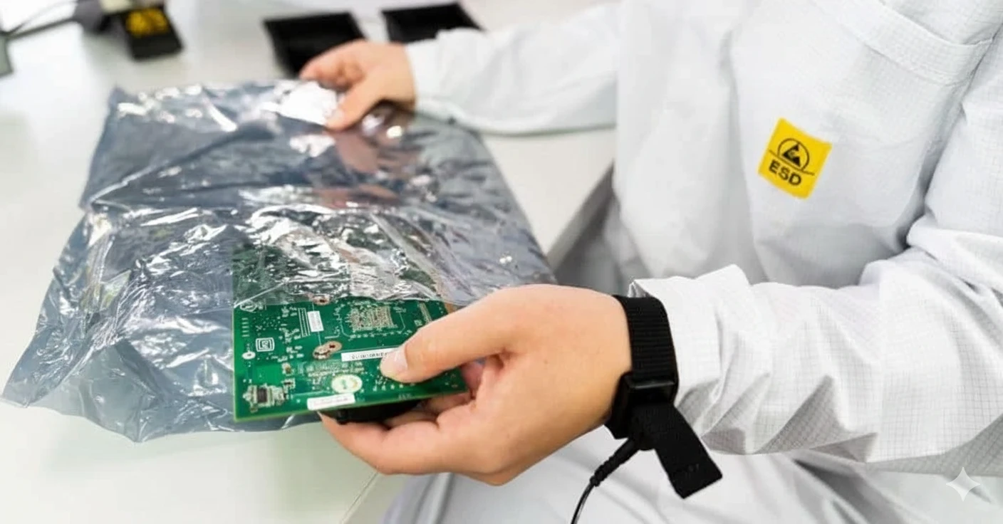
Person handling a circuit board beside a silver antistatic bag
Protective handling and material identification continue from receipt through assembly.

PCB Inspection

Checking dimensions, hole sizes, copper thickness, solder mask, and character printing; verifying no scratches, warping, or delamination.

Component Inspection

Verifying model, brand, batch, date codes, packaging, and any signs of defects like pin oxidation, bending, or contamination. For key components (e.g., MOSFETs, ICs), we may perform electrical performance testing to ensure conformity to specifications.

04 / In-process control

Inspect the print and placement while correction is still local.

1) Solder Paste Inspection (SPI)

3D SPI measures thickness, volume, area, and alignment to detect underprinting, excess paste, misalignment, and bridging.

2) Pre-reflow Inspection (AOI)

Checks correct placement, orientation, polarity, types, and missing or misplaced parts before reflow to prevent rework.

3) Reflow Soldering & Wave Soldering Control

Lead-free profiles (e.g., SAC305), multiple reflow passes for double-sided SMT, and controlled wave soldering; every curve is documented for traceability.

05 / Solder-joint evidence

Choose visible and hidden-feature inspection deliberately.

Scope note Define the packages, detectable features and acceptance rules for each inspection method. Difficult findings may need another view or confirmation method.
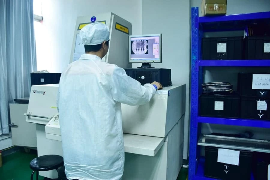
Operator viewing circuit board X-ray images at an inspection workstation
X-ray inspection requires a defined viewing method, target feature and acceptance rule.

AOI (Automatic Optical Inspection) Post-reflow

High-speed cameras identify misalignment, solder bridges, missing components, and incorrect polarity—crucial for medium-to-large batches and complex BOMs.

X-Ray Inspection (AXI) for Hidden Solder Joints

For BGA, QFN, CSP, and hidden joints, AXI detects voids, bridges, cold joints, misalignments, and pad/ball fusion quality.

06 / Test & final release

Connect electrical checks, final condition and release records.

Add electrical and functional evidence.

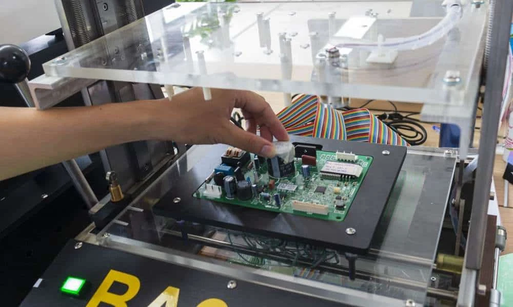
Operator connecting a populated circuit board on an electrical test fixture
Electrical and functional checks follow the scope agreed for the build.

ICT (In-Circuit Testing)

For high-volume or mission-critical builds, checks components and connections for shorts/opens, tolerances, and accurate connectivity.

FCT (Functional Circuit Testing)

Simulates operational environments—voltage/current/frequency checks, I/O and interface tests (USB, Ethernet, UART), and peripherals like buttons, LEDs, sensors.

Burn-in Testing

Stresses PCBAs under high temperature, humidity, and power to surface early failures for high-reliability products (industrial, medical, telecom).

Complete the inspection and cleaning route.

After all testing, experienced quality personnel check cosmetic defects, cleanliness (flux residues, fingerprints), and structural integrity. Boards are then cleaned with IPA or other agents to ensure the PCBA is free from contaminants.

Review your current coverage.

Get in Touch with APTPCB for Reliable PCBA Quality Testing Services

If you need a trusted partner for PCB manufacturing and PCBA assembly with top-notch quality control and testing services, we can:

By partnering with APTPCB, you ensure your products meet and exceed the highest standards of reliability and performance, ready to thrive in the marketplace.

  • Assess the current testing coverage of your product.
  • Provide customized PCBA quality testing solutions.
  • Offer competitive quotes and delivery timelines.

ENGINEERING REFERENCE

Additional quality-system capabilities and supplier context

Connect the inspection chain and records.

Comprehensive Integration

Quality testing embedded through the entire PCB manufacturing and assembly process for a one-stop solution.

State-of-the-art Testing Equipment

SPI, AOI, AXI, ICT, FCT, and burn-in testing to ensure thorough assurance.

Experienced Quality Team

IPC-certified engineers and technicians skilled in failure analysis and process optimization.

Traceability

Robust traceability from component batch to production lot for full visibility.

Customizable Testing Solutions

Tailored validation per product needs, including custom functional and aging tests.

PRACTICAL QUESTIONS

Before you release the work.

What happens during design evaluation for PCBA quality?
We perform DFM and DFT reviews plus PCB layering/routing/test point suggestions to catch risks early and ease manufacturing and testing.
How do you control incoming quality before production?
We inspect PCB dimensions, holes, copper, solder mask, print, and surface condition, and verify components for model, brand, batch, date code, packaging, and defects; key parts can receive electrical performance checks.
Which inline process controls do you apply?
3D SPI for paste volume/alignment, pre-reflow AOI for placement and polarity, and tuned reflow/wave soldering profiles with documented curves for traceability.
How do you inspect hidden solder joints like BGAs?
Post-reflow AOI handles visible joints, and X-ray (AXI) checks hidden BGA/QFN/CSP joints for voids, bridges, cold joints, misalignment, and pad/ball fusion quality.
What functional and reliability tests are available?
ICT for shorts/opens and component values, FCT for real-world functions and interfaces, and burn-in to stress boards for high-reliability applications.
What does electronics manufacturing quality control cover?
Quality control connects incoming material checks, process inspection and final release to the approved design and acceptance criteria. Define required records, traceability and how nonconformances or changes are approved.
How should IPC requirements be specified in an order?
IPC documents address different tasks, including board performance, visual acceptance and assembly workmanship. Specify the applicable document, revision, class and any agreed exceptions rather than requesting a generic IPC certification.

ENGINEERING & PRODUCTION REVIEW

Review the inspection chain for your product.

Bring the existing test strategy and identify the evidence needed for release.

  • Gerber / CAD and approved BOM
  • Product functions and interface test requirements
  • Critical packages and reliability targets
  • Acceptance criteria and traceability requirements