
1+N+1
Single build-up per side
One sequential build-up layer is added on each side of a conventional core. Release the laser-via diameter, capture pad, target layer, fill requirement, and copper finish with the stack-up.

Layer construction before routing release
A PCB stack-up is the ordered construction of copper layers, cores, prepregs, and special materials that determines reference planes, routing space, finished thickness, impedance geometry, and fabrication sequence. APTPCB reviews stack-ups against material, lamination, drilling, plating, thermal, and test requirements before production release.
Engineering foundation
Layer count alone does not define a manufacturable stack-up. The design must connect signal layers to stable reference planes, allocate dielectric spacing for impedance, provide enough copper and resin balance for lamination, and reserve a realistic drill and plating path. Early review with impedance-control requirements reduces late geometry changes.
APTPCB reviews the proposed construction against the verified 4–32 layer rigid-board range, material availability, finished thickness, copper weights, via types, sequential-lamination needs, and required evidence. The approved output should be a releaseable layer table rather than an informal sketch.
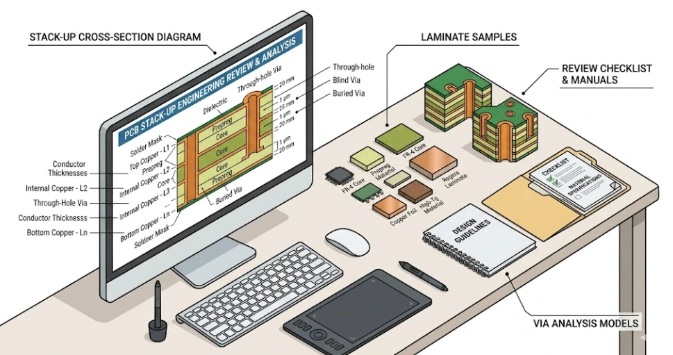
Architecture selection
This comparison separates architectures by fabrication sequence and design input rather than treating every multilayer board as the same construction.
| Architecture | Typical use | Construction decision | Main release inputs | Primary risk to review |
|---|---|---|---|---|
| Rigid FR-4 multilayer | Industrial control, computing, instrumentation | Through-hole or selected blind/buried structure | Layer order, copper, thickness, material class | Plane reference, balance, drill aspect ratio |
| Low-loss digital multilayer | High-speed links and dense computing | Low-loss material and copper profile selected by channel need | Loss target, stack-up, impedance table, routing constraints | Material substitution and insertion-loss margin |
| HDI sequential build | Fine-pitch fan-out and compact routing | One or more sequential lamination cycles | Microvia layers, capture pads, fill and plating needs | Registration, stacked versus staggered vias, cycle count |
| Flex or rigid-flex | Folded interconnects and space-constrained assemblies | Polyimide flex zones joined to rigid areas as specified | Bend region, coverlay, stiffener, layer transitions | Bend reliability and transition geometry |
| Heavy-copper or thermal build | Power conversion and thermal spreading | Copper distribution and dielectric system chosen together | Current, copper weight, spacing, thermal path | Resin fill, etch capability, thickness variation |
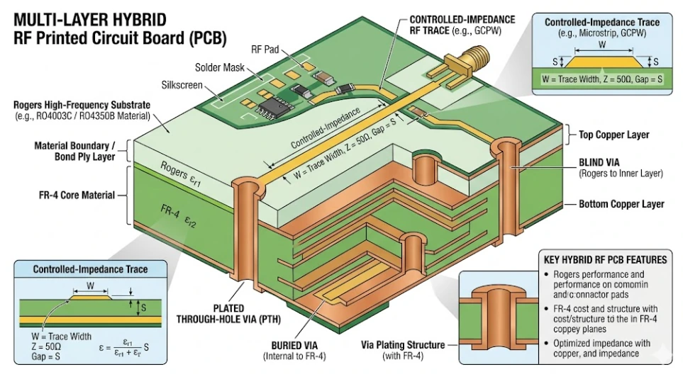
| RF or mixed-material build | RF front ends, antennas, mixed RF/digital boards | RF laminate used only where electrical need justifies it | Frequency, Dk/Df need, copper type, bond layer | Material compatibility, registration, thickness tolerance |
Architecture feasibility depends on the complete construction. Material names, via schemes, and thicknesses remain provisional until the fabrication data and acceptance requirements are reviewed.
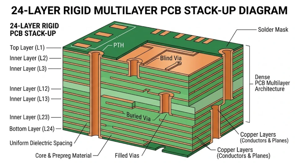
Rigid multilayer
A rigid multilayer stack-up should give critical signals a defined reference while keeping copper distribution and dielectric construction reasonably balanced around the board center. Plane assignment, split planes, return paths, and routing transitions matter as much as the nominal number of layers.
As layer count increases within the 4–32 layer range, drill depth, registration, lamination sequence, finished thickness, and test access become stronger constraints. Back-drilling, buried vias, or special materials should be justified by an electrical or mechanical requirement and released with clear tolerances.
HDI sequence
HDI feasibility depends on which layers connect, how microvias are formed and filled, and how many lamination cycles the design requires.
One sequential build-up layer is added on each side of a conventional core. Release the laser-via diameter, capture pad, target layer, fill requirement, and copper finish with the stack-up.
Two build-up layers increase routing access but add alignment and process dependencies. Confirm HDI fabrication boundaries, then state whether microvias are staggered or stacked and whether copper filling is required.
Document every blind, buried, and through-hole span. Avoid ambiguous via labels that do not identify start layer, stop layer, finished size, or fill and cap requirements.
Approve the proposed lamination sequence, material set, microvia structure, impedance construction, and any microsection or registration evidence before tooling release.
Flex and rigid-flex
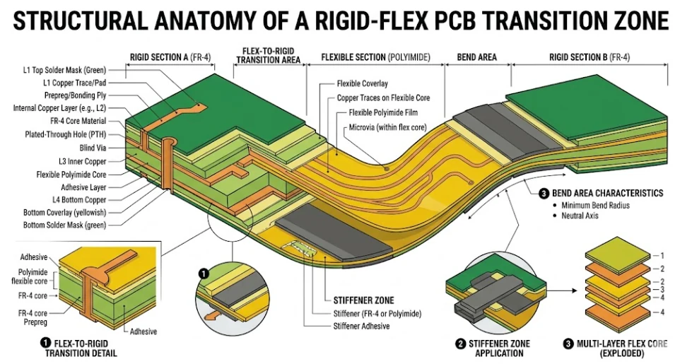
A flex or rigid-flex construction must identify which layers continue through the bend, where coverlay and stiffeners begin, how copper is oriented, and whether the bend is static or dynamic. The flex zone should not inherit rigid-board assumptions about dielectric, mask, or via placement.
Release the bend radius, flex thickness, copper type, transition geometry, stiffener locations, and assembly constraints. Review related flex PCB capability boundaries before the mechanical enclosure freezes the routing path.
Power and thermal
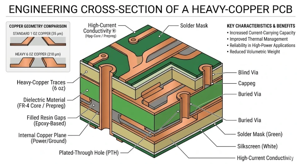
A heavy-copper construction changes spacing, etching, resin fill, pressed thickness, and drill planning. Define the actual current path, copper distribution, voltage spacing, finished copper need, and allowable temperature rise instead of selecting copper weight by a generic rule.
Metal-core and other thermal constructions require the dielectric layer, thermal path, isolation need, base material, thickness, and mechanical attachment to be reviewed as one system. Thermal PCB requirements should be separated from signal-layer stack-up assumptions.
RF and mixed materials
A mixed RF and digital stack-up can reduce material use, but it introduces compatibility questions: dielectric properties, copper profile, bond layer, thermal expansion, drilling behavior, registration, and pressed thickness must work together. The material name alone does not define the finished electrical structure.
Provide operating frequency, impedance, loss objective, RF layer, reference plane, copper requirement, finish, environmental exposure, and mechanical tolerance. Review available RF laminate options only after the required properties are clear.
Release-input matrix
Each input changes more than one downstream process, so review them as a connected release package.
| Input | What to provide | Manufacturing effect | Release evidence |
|---|---|---|---|
| Layer order | Signal, plane, power, and reference assignment | Imaging, lamination, drill map | Approved layer table |
| Material system | Named material or property requirement and substitution rule | Press cycle, drilling, electrical behavior | Approved material set |
| Copper | Starting and finished copper by layer | Etching, plating, resin fill, thickness | Copper table in stack-up |
| Dielectric spacing | Target spacing or impedance-driven construction | Pressed thickness and impedance geometry | Reviewed core/prepreg construction |
| Via structure | Start/stop layers, size, fill, cap, back-drill | Drilling, plating, lamination sequence | Released via map |
| Finished thickness | Nominal value and tolerance | Material selection and press construction | Approved stack-up thickness |
| Verification | Impedance, microsection, dimensional, or other reports | Coupon and inspection planning | Defined shipment record list |
Upload the proposed layer table, thickness, material requirements, copper weights, impedance table, via map, fabrication constraints, and Gerber X2, ODB++, or IPC-2581 data for engineering review.
A core is a cured dielectric sheet with copper on one or both sides. Its thickness is comparatively stable and it often forms the starting image layers in a multilayer construction.
A prepreg contains partially cured resin and reinforcement. During lamination it bonds adjacent layers and flows around copper features; final pressed thickness depends on the prepreg construction, resin content, copper distribution, and press process.
For that reason, substituting one core or prepreg style can change total thickness, resin fill, impedance geometry, and material behavior. Substitution rules belong in the approved release, not in an informal purchasing note.
Start with operating temperature, electrical loss, frequency, thermal expansion, flammability requirement, moisture exposure, thickness tolerance, copper profile, and assembly process. A brand name without these constraints leaves substitution and availability risk unresolved.
For conventional multilayers, FR-4 families may satisfy the need when Tg, decomposition behavior, loss, and CAF expectations are defined. High-speed or RF layers may require lower-loss materials, while flex zones require polyimide constructions and coverlay-compatible processing.
The quotation should identify the proposed material set and any allowed equivalents. If an exact grade is mandatory, state it explicitly and account for sourcing lead time before the production date is committed.
References should be selected for the actual construction and contract: IPC-2221 for generic design, IPC-2226 for HDI, IPC-6012 for rigid boards, and IPC-6013 for flexible or rigid-flex boards. State the class, acceptance criteria, and required reports explicitly in the fabrication drawing.
Assign signal, plane, and power layers so critical routes have continuous return paths. Identify split-plane crossings and layer transitions before the routing density consumes the available space.
Review copper distribution, core and prepreg placement, and mechanical symmetry. Balance is an engineering check, not simply an equal number of layers above and below the center.
State every through, blind, buried, filled, capped, and back-drilled structure with start layer, stop layer, finished size, tolerance, and special processing requirement.
List target impedance, tolerance, layer, trace type, and reference plane. Approve geometry changes caused by the reviewed dielectric construction before fabrication.
State required material properties, exact grades where mandatory, allowed substitutions, finished thickness, copper definition, and any property that must be reported with shipment.
Provide release-ready fabrication data in Gerber X2, ODB++, or IPC-2581 format, plus drill data, proposed layer order, board thickness and tolerance, copper by layer, material requirements, impedance table, via map, critical dimensions, quantity, and required verification reports.
Application-driven construction
Prioritize uninterrupted return paths, via transitions, material loss, copper profile, impedance tolerance, and the evidence required for critical channels.
Prioritize Dk/Df need, copper roughness, bond layer, RF reference planes, finish, mechanical tolerance, and separation from noisy digital or power regions.
Prioritize current path, voltage spacing, copper distribution, resin fill, isolation, heat spreading, assembly temperature, and mechanical attachment.
Prioritize fine-pitch escape, microvia sequence, bend region, flex thickness, stiffeners, component keep-outs, enclosure clearance, and assembly handling.
Stack-up FAQ
Remote engineering review
Keep layer, material, impedance, via, and thickness decisions in one reviewable release package across locations and suppliers.
Release reference planes, loss needs, impedance structures, via transitions, back-drill requirements, and channel evidence before routing sign-off.
Release material restrictions, traceability, thickness tolerance, acceptance criteria, change rules, and the reports required for design records.
Keep the same approved construction tied to tooling, panelization, impedance coupons, and repeat-order data when quantities or factories change.
Release material properties, RF reference structures, environmental limits, special inspection, and final system responsibility before quotation.
Upload the proposed layer table, board thickness, copper weights, material requirements, impedance table, via map, Gerber X2, ODB++, or IPC-2581 data, and required reports.