FLEX CIRCUITS

Flexible PCB Manufacturing — Polyimide & LCP Experts

Flexible circuits built on adhesive-less polyimide or LCP cores with rolled-annealed copper, laser-drilled coverlay relief, and cleanroom SMT carriers for medical, wearable, aerospace, and industrial assemblies.

  • Adhesive-less PI & LCP stack-ups
  • Rolled-annealed Cu 12.5–105 µm
  • Coverlay laser relief & hatched grounds
  • Cleanroom SMT with carriers
  • FR4 / PI / stainless stiffeners
  • 1M-cycle bend validation

Get an Instant Quote

Full Quote →

Flexible PCB Turnkey Manufacturing & Assembly

APTPCB engineers translate ODB++ or IPC-2581 into bend-aware stack-ups, selecting adhesive-less polyimide or LCP cores, rolled-annealed copper weights, and impedance meshes that survive flex-to-install and dynamic zones.

We integrate coverlay relief windows, FR4/PI/stainless stiffeners, PSA, and selective plating so connector fingers, sensors, and LEDs stay flat while bend sections remain compliant.

Cleanroom SMT fixtures, carriers, and handling work instructions keep 01005 assemblies, fine-pitch BGAs, and camera modules aligned through reflow, forming a single workflow from prototype through scaled production.

APTPCB's Flex Manufacturing Guide documents the 17 touchpoints we run on every lot—from PI/PET pre-clean, NC drilling, electroless copper, dry-film lamination, LDI exposure, develop/etch/strip, and AOI through coverlay layup, drilling, ENIG, legend, electrical test, stiffener bonding, routing, FQC, and vacuum-sealed pack-out. That cadence keeps every panel traceable.

The same guide contrasts single-sided and double-sided flex flows: single-sided builds emphasize material cutting and coverlay window control, while double-sided circuits manage RA copper grain direction, hatched grounds, adhesive stacks, and shared stiffeners. We reuse those best practices when co-engineering stack-ups for wearables, medical devices, and camera modules.

Flexible PCB Turnkey Manufacturing & Assembly

Flexible Circuit Programs We Build

Representative projects across wearables, medical devices, automotive cabins, aerospace harnesses, and industrial equipment.

Foldable display harnesses

Foldable display harnesses

Wearable sensor loops

Wearable sensor loops

Medical probes & catheters

Medical probes & catheters

Camera & imaging modules

Camera & imaging modules

Satellite & UAV harness

Satellite & UAV harness

Rigid-flex control panels

Rigid-flex control panels

High-Reliability Flex & Rigid-Flex Builds

We pair IPC-2223 design practice with coverlay relief, controlled copper balancing, and 100% electrical plus bend validation so every flex tail, hinge, and connector zone survives installation and life testing.

Download Capabilities
Polyimide / LCP coresRolled-annealed copperCoverlay laser reliefCleanroom SMT carriersFR4 / PI / stainless stiffeners1M-cycle bend logs

APTPCB Flexible Circuit Manufacturing Services

We support single- and multi-layer flexible circuits, rigid-flex hybrids, and ultra-thin harness replacements with full DFx collaboration, stack-up modeling, and assembly support.

Flexible Circuit Constructions

Select the right combination of flex layers, dielectric thickness, copper weights, and stiffeners to balance bend performance, impedance, and assembly stability.

  • Single-Sided Flex – Ultra-thin jumpers and LED tails with one copper layer, coverlay protection, and optional stiffeners under components.
  • Double-Sided Flex – Signal and return layers connected with microvias or button-plated PTH for impedance-controlled sensor links.
  • Multilayer Flex – Four or more flex layers with embedded mesh grounds for RF, camera modules, and foldable displays.
  • Rigid-Flex – Flex cores laminated to FR4 or high-Tg rigid sections to host connectors, BGAs, or high-power components while routing flex tails through hinges.
  • Hybrid Flex Assemblies – Flex plus heater films, shield foils, or integrated stiffeners for aerospace harness and medical probes.

Interconnect & Bend Features

  • Laser-Skived Coverlay Relief: Windowing coverlay around pads maintains coplanarity and impedance.
  • Button-Plated PTH: Copper button plating reinforces vias transitioning between flex and stiffener zones.
  • Microvias & Blind Vias: Used in rigid-flex build ups to keep bend areas free of copper stacks.
  • Hatched Ground Mesh: Lightweight reference planes preserve impedance without adding stiffness.
  • Shield Films & Copper Foil: Applied selectively for EMI control in medical and RF probes.
  • Stiffener Step-Downs: Controlled depth routing and chamfers reduce stress where flex meets FR4.

Sample Flex & Rigid-Flex Stack-Ups

  • 1 Layer Flex: 25 µm PI + 18 µm RA Cu with 12 µm coverlay, ideal for flex-to-install jumpers.
  • 2 Layer Flex Impedance: 35 µm RA Cu / 50 µm PI / 35 µm RA Cu with hatched ground and coverlay relief for differential pairs.
  • 6 Layer Rigid-Flex (2F + 2R + 2F): Flex cores laminated to FR4, sharing microvia stacks for cameras, aerospace, or instrumentation harnesses.

Material and Design Guidelines

Adhesive-less polyimide, LCP cores, and RA copper support tight bends. Coverlay relief, hatched grounds, and copper balancing protect impedance and prevent work hardening.

  • Use adhesive-less PI 12–50 µm or LCP for dynamic regions to prevent copper peel.
  • Select RA copper ≤ 35 µm for hinges; thicker ED copper reserved for power flex jumpers.
  • Avoid plated vias inside bend zones; stagger traces at 45° and keep neutral axis centered.
  • Relieve coverlay and hatched grounds to maintain impedance while minimizing stiffness.

Reliability & Validation

Dynamic bend fixtures, 1M-cycle logging, thermal shock, and micro-section analysis verify copper grain direction, adhesion, and stiffener bond strength before release.

Cost & Application Recommendations

  • Single-sided flex jumpers: Lowest cost when components live on supporting FR4 or stiffeners.
  • Double-sided impedance flex: Balances routing density with manageable lamination cycles for sensors and cameras.
  • Hybrid rigid-flex: Use rigid sections only under components to control lamination count and assembly cost.

Flexible Circuit Build Flow

1

Data Intake & DFx

Review ODB++ / IPC-2581 within 24 hours, flag bend zones, impedance pairs, and stiffener stack-ups.

2

Stack-Up & Coverlay Design

Model PI/LCP thickness, copper weights, meshes, and relief windows matched to bend profile.

3

Imaging & Etch

LDI defines 50/50 µm traces while copper balancing keeps dynamic regions uniform.

4

Pre-Clean & NC Drilling

Following the APTPCB playbook, PI/PET rolls receive plasma plus scrub cleaning before high-precision NC drilling sets datum holes and future copper registration.

5

Electroless Copper & LDI Imaging

After mass electroless copper, we laminate photoresist, run LDI for 50/50 μm traces, and complete develop/etch/strip exactly as captured in steps 3–6 of the guide.

6

Coverlay, Stiffeners & Finish

Steps 8–17 govern coverlay layup/lamination, drilling, ENIG, legend, electrical test, FR4/PI/stainless stiffeners, routing, and FQC with vacuum sealing—our travelers record the same sequencing per lot.

7

SMT & Validation

Cleanroom SMT, selective solder, and bend cycling up to 1M cycles confirm mechanical and electrical reliability.

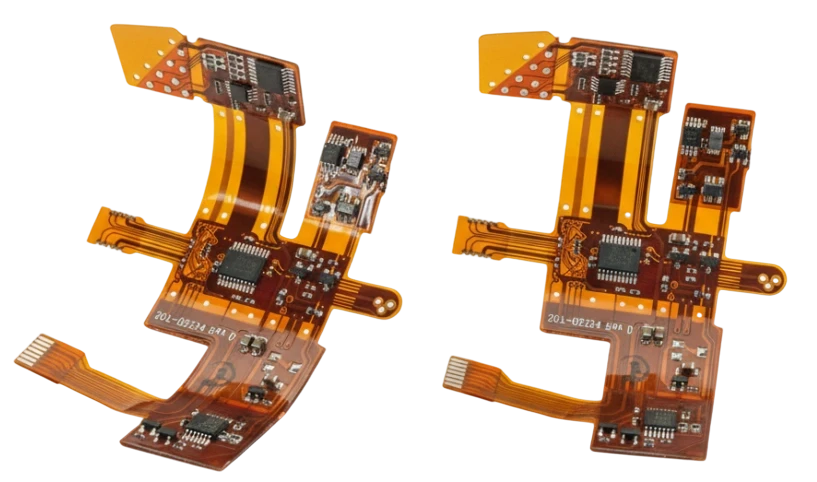
Flex CAM Engineering & DFx Review

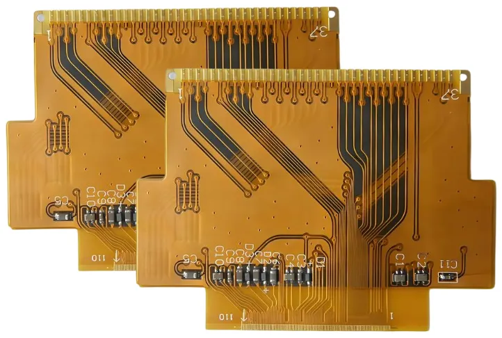
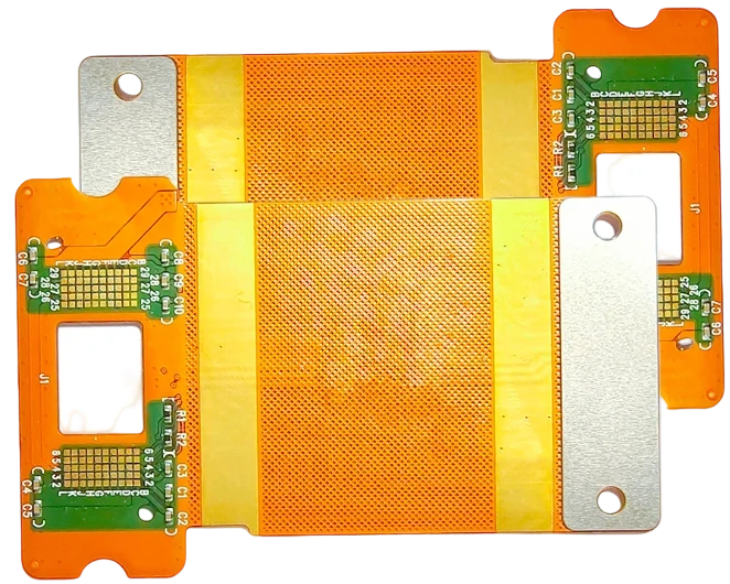
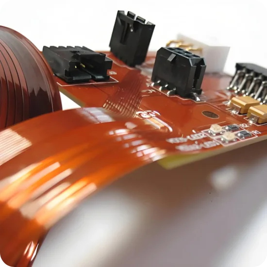
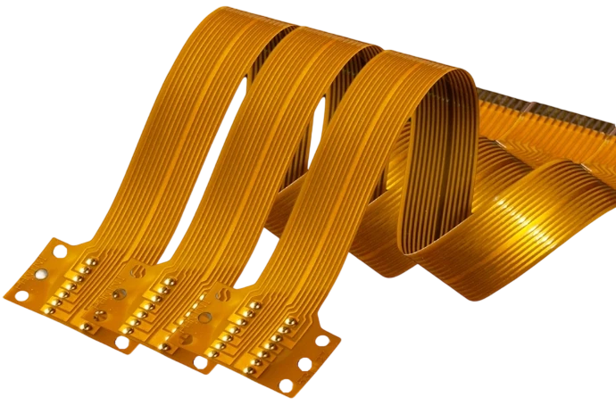
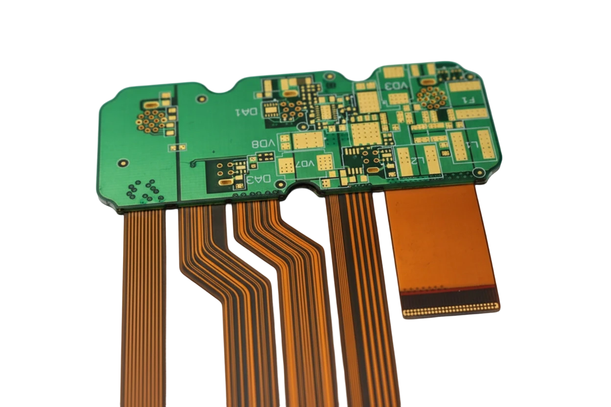
CAM engineers extract bend stack-ups, impedance targets, and stiffener callouts from ODB++ files, then create relief patterns, hatched grounds, and carrier tooling before routing to production.

  • Verify bend zones, neutral axis placement, and keep-out regions before tooling.
  • Confirm stack-up thickness, copper grain direction, and impedance meshes for each layer.
  • Generate coverlay relief, hatched grounds, and tear-stop features.
  • Define stiffener outlines, PSA windows, and depth-controlled rout paths.
  • Annotate impedance coupons, dynamic test coupons, and handling instructions.
  • Optimize panel utilization with shared carriers and fiducials for SMT.
  • Release fabrication notes covering bake cycles, cleanroom requirements, and packaging method.

Manufacturing Execution & Feedback Loop

Process engineers monitor imaging, lamination, and forming windows with SPC dashboards, feeding bend data and copper thickness measurements back to CAM to refine future panels.

  • Control lamination pressure and temperature to avoid resin squeeze-out in flex cores.
  • Monitor LDI alignment and etch balance to keep 50/50 µm geometries within tolerance.
  • Inspect coverlay bonding, relief accuracy, and adhesive flow around pads.
  • Validate stiffener planarity and PSA cure before singulation.
  • Run bend and tensile sampling per lot with logged displacement and resistance data.
  • Perform AOI, flying probe, and optical inspection to confirm routing and spacing.
  • Package finished flex with protective carriers and humidity indicators to prevent creasing.
50/50 µm

Lines / Spaces

LDI on adhesive-less PI

≥6×

Flex Bend Radius

Static flex-to-install guideline

1M cycles

Dynamic Testing

Bend validation reports

01005

Assembly Pitch

Cleanroom SMT carriers

Advantages of Flexible PCBs

Replace wire harnesses and connectors with lighter, more reliable flex circuits.

Harness Replacement

Eliminate bulky wire harnesses with ultra-thin flex tails that reduce weight by up to 70%.

Integrated Stiffeners

Bond FR4, PI, or stainless stiffeners exactly where components need support while keeping bend zones compliant.

RF & High-Speed Ready

Controlled impedance meshes, hatched grounds, and LCP cores maintain ±5% targets for antennas and sensors.

Validated Reliability

Bend, vibration, and thermal stress testing prevent copper work hardening before systems ship.

Design Freedom

Route in 3D space, wrap housings, and connect rotating modules without sacrificing performance.

System-Level Savings

Lower part counts, fewer connectors, and simplified assembly reduce total cost of ownership.

Manufacturing Simplified

Shared panel tooling, SMT carriers, and ECN governance keep builds fast from prototypes to volume.

Traceable Validation

Bend logs, moisture control records, and IPC 6013 Class 3 inspection provide clear audit trails.

Why Choose APTPCB?

Flex circuits fold, wrap, and hinge without sacrificing impedance or signal integrity, enabling smaller enclosures and faster assembly.

WearablesMedical probesFoldable devicesCamera modulesAerospace harnessIndustrial automation
APTPCB production line
Adhesive-less PI flex line

Flex PCB Applications

Deploy flexible circuits where weight, bend profile, or constrained enclosures rule out rigid boards.

From foldable displays to surgical tools and satellites, flex circuits streamline wiring, shorten signal paths, and harden products against vibration.

Wearables & Consumer

Low-profile flex tails for smartwatches, AR/VR headsets, and foldable phones.

SmartwatchesVR strapsFoldablesAudioCameras

Medical & Life Sciences

Sterilizable flex circuits inside catheters, imaging probes, and patient monitors.

CathetersEndoscopyImagingDiagnosticsWearable therapy

Aerospace & Defense

Lightweight harness replacements qualified for vibration and temperature extremes.

SatellitesUAVRadarCockpitMissile

Automotive Interiors

Slim flex circuits integrate lighting, sensors, and HMI controls inside EV cabins.

HUDADASAmbient lightingSeatsBattery sensing

Industrial Automation

Flexible jumpers bridge motion axes, robots, and inspection tools under constant movement.

RoboticsCobotsInspectionPackagingFactory IoT

Telecom & RF

LCP-based flex for beam-forming antennas, phased arrays, and filter modules.

5GSatcomFiltersBeam-formingIoT gateways

Instrumentation & Sensors

Precision sensors, lidar, and measurement tools rely on stable, lightweight flex.

LidarMicroscopesSecurityIndustrial sensingScientific

Computing & Displays

Camera modules, foldable displays, and high-density connectors need tight pitch flex.

CamerasDisplaysModulesFoldablesStorage

Flex PCB Design Challenges & Solutions

Managing bend reliability, impedance control, and assembly handling requires cross-functional collaboration between design, CAM, and manufacturing teams.

Common Design Challenges

01

Copper Work Hardening

Repeated bending can crack copper if grain direction, thickness, or plating is not matched to the bend radius.

02

Coverlay & Impedance Balance

Improper relief openings or hatched grounds change impedance and raise stiffness around pads.

03

Stiffener Alignment

Misaligned FR4 or stainless stiffeners create stress risers that delaminate under thermal cycling.

04

Handling & Assembly Damage

Thin flex tails can crease or scratch during SMT unless carriers and instructions are provided.

05

Moisture & Cleanliness

Polyimide absorbs moisture, causing blowouts during reflow without proper baking and packaging.

06

Transitioning to Rigid Sections

Poorly managed rigid-flex transitions cause resin cracks and trace neckdowns that fail in test.

Our Engineering Solutions

01

Bend Modeling & Neutral Axis Control

We align copper grain direction, use staggered traces, and adjust dielectric thickness so the neutral axis stays centered through each hinge.

02

Precision Coverlay Processing

Laser-drilled or routed openings expose pads without overhang, while relief slots maintain consistent impedance.

03

Stiffener Tooling & PSA Selection

Dedicated tooling holes and PSA thickness control keep stiffeners registered within ±0.05 mm.

04

Carrier & Fixture Design

Custom stainless or FR4 carriers with clamp bars, kapton tapes, and fiducials protect flex circuits during SMT and test.

05

Environmental Conditioning

Pre-bake, nitrogen storage, and desiccant packaging remove moisture so flex tails survive reflow and global shipping.

How to Control Flex PCB Cost

Flex circuits become expensive when stack-ups are thicker than needed, stiffeners span the entire outline, or coverlay tooling requires extra passes. Designing for manufacturability — right copper weights, simplified stiffener counts, and shared carriers — keeps prototyping fast and production predictable. Send intended bend radii, material preferences, and assembly plans with your data. Early DFx review often cuts lamination cycles, stiffener layers, and tooling changes before build.

01 / 08

Match Copper Weight to Function

Use thin RA copper in dynamic zones and limit thicker ED copper to power jumpers to avoid rework.

02 / 08

Panelize for Shared Carriers

Design flexible coupons and break-off tabs so multiple part numbers share one SMT carrier set.

03 / 08

Align Surface Finish with Need

ENIG suits most flex builds; reserve ENEPIG or immersion silver for mixed wire-bond applications.

04 / 08

Limit Stiffener Count

Combine component areas onto shared FR4 islands so lamination and PSA steps stay efficient.

05 / 08

Define Acceptable Bend Classes

Clarify which zones are dynamic vs. install-only to avoid over-specifying copper fill or testing.

06 / 08

Co-Engineer Stack-Ups Early

Sharing PI thickness and bend targets before layout saves respins and accelerates NPI.

07 / 08

Use Standard Coverlay Thickness

25–50 µm PI coverlay with common drill sizes reduces tooling passes and scrap.

08 / 08

Consolidate Rigid Sections

Place BGAs and connectors on a single rigid block instead of multiple, reducing lamination cycles.

Certifications & Standards

Quality, environmental, and industry credentials supporting reliable manufacturing.

Certification
ISO 9001:2015

Quality management for flex manufacturing and SMT.

Certification
ISO 14001:2015

Environmental controls for chemical processing and adhesives.

Certification
ISO 13485:2016

Traceability and cleanliness for medical flex assemblies.

Certification
IATF 16949

Automotive PPAP, bend validation, and CAPA coverage.

Certification
AS9100

Aerospace-grade process governance for flex builds.

Certification
IPC-6013 / 600

Flexible circuit performance and acceptance criteria.

Certification
UL 94 V-0 / UL 796

Safety compliance for global shipments.

Certification
RoHS / REACH

Hazardous substance compliance.

Selecting a Flex PCB Manufacturing Partner

  • Experience with IPC-2223 design and IPC-6013 Class 3 inspection.
  • Adhesive-less PI and LCP sourcing with traceability.
  • Cleanroom SMT, selective solder, and fixture design in-house.
  • Dedicated bend, tensile, and environmental test equipment.
  • Ability to scale from prototypes to mass production without changing factories.
  • Multilingual engineering support with 24-hour DFx feedback.
Selecting a flex PCB manufacturing partner

Quality & Cost Console

Process & Reliability Controls + Economic Levers

Unified dashboard connecting HDI quality checkpoints with the economic levers that compress cost.

Process & Reliability

Pre-Lamination Controls

Stack-Up Validation

  • Panel utilization+5–8%
  • Stack-up simulation±2% thickness
  • VIPPO planningPer lot
  • Material bake110 °C vacuum

Pre-Lamination Strategy

• Rotate outlines, mirror flex tails

• Share coupons across programs

• Reclaim 5-8% panel area

Registration

Laser & Metrology

Registration

  • Laser drill accuracy±12 μm
  • Microvia aspect ratio≤ 1:1
  • Coverlay alignment±0.05 mm
  • AOI overlaySPC logged

Laser Metrology

• Online laser capture

• ±0.05 mm tolerance band

• Auto-logged to SPC

Testing

Electrical & Reliability

Testing

  • Impedance & TDR±5% tolerance
  • Insertion lossLow-loss verified
  • Skew testingDifferential pairs
  • Microvia reliability> 1000 cycles

Electrical Test

• TDR coupons per panel

• IPC-6013 Class 3

• Force-resistance drift logged

Integration

Assembly Interfaces

Integration

  • Cleanroom SMTCarrier + ESD
  • Moisture control≤ 0.1% RH
  • Selective materialsLCP / low Df only where needed
  • ECN governanceVersion-controlled

Assembly Controls

• Nitrogen reflow

• Inline plasma clean

• 48h logistics consolidation

Architecture

Stack-Up Economics

Architecture

  • Lamination cyclesOptimize 1+N+1/2+N+2
  • Hybrid materialsLow-loss where required
  • Copper weightsMix 0.5/1 oz strategically
  • BOM alignmentStandard cores first

Cost Strategy

• Balance cost vs performance

• Standardize on common cores

• Low-loss only on RF layers

Microvia Planning

Via Strategy

Microvia Planning

  • Staggered over stacked-18% cost
  • Backdrill sharingCommon depths
  • Buried via reuseAcross nets
  • Fill specificationOnly for VIPPO

Via Cost Savings

• Avoid stacked microvias

• Share backdrill tools

• Minimize fill costs

Utilization

Panel Efficiency

Utilization

  • Outline rotation+4–6% yield
  • Shared couponsMulti-program
  • Coupon placementEdge pooled
  • Tooling commonalityPanel families

Panel Optimization

• Rotate for nesting efficiency

• Share test coupons

• Standardize tooling

Execution

Supply Chain & Coating

Execution

  • Material poolingMonthly ladder
  • Dual-source PPAPPre-qualified
  • Selective finishENIG / OSP mix
  • Logistics lanes48 h consolidation

Supply Chain Levers

• Pool low-loss material

• Dual-source laminates

• Match finish to need

Flexible PCB Manufacturing — Upload Data, Get a Build Plan

Talk to Flex Engineering
IPC-2223 / IPC-6013 compliance
Cleanroom SMT and fixtures
Adhesive-less PI & LCP inventory
Prototype to volume in one flow

Share stack-ups, bend targets, and assembly details — our flex engineering desk replies with DFx notes, lead time, and costing within one business day.

Flex PCB FAQs

Guidance on bend radii, materials, impedance control, and assembly handling.