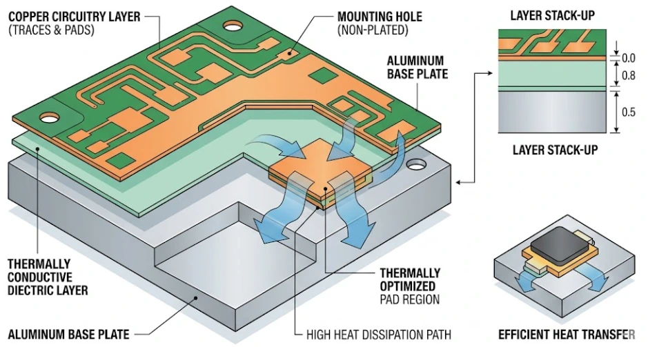
| Aluminum MCPCB | Al 5052 / 6061 base, Bergquist / Laird / Ventec / Totking IMS and equivalents | 1.0–3.0 W/mK, 1–4 layers, up to 43.3" × 19" | LED lighting, power supplies, motor drives |
| Copper MCPCB | Cu C11000 base, premium IMS dielectric | 3.0–8.0+ W/mK, 1–4 layers | High-power LED, RF PA, IGBT modules, EV power |
| Iron-Base MCPCB | Fe base plate, thermally conductive dielectric | Mechanical strength + thermal management | Automotive power modules, industrial motor drives |
| Ceramic PCB | Al₂O₃ (Alumina), AlN (Aluminum Nitride) | 24–170 W/mK, DBC/DPC/LTCC | Power modules, sensors, high-temp, space, laser diodes |
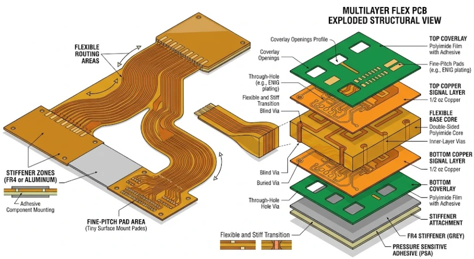
| Flex PCB | Polyimide — DuPont Pyralux, Panasonic Felios, Shengyi, Taiflex, Doosan, and equivalents | 1–8 layers, RA/ED copper, coverlay | Wearables, medical, automotive, FPC cables |
| Rigid-Flex PCB | FR-4 rigid + PI flex, adhesiveless and adhesive construction | Up to 32 layers, 2/2 mil, bookbinder | Smartphones, aerospace, medical implants, avionics |
| Gold Finger PCB | Standard FR-4, high-Tg, or specialty substrates | Hard gold 0.5–2.5 μm over 3–5 μm Ni, beveled | Edge connectors, test cards, memory modules, PCIe/DDR slots |
| Carbon Ink PCB | Standard FR-4 with screen-printed carbon | Printed carbon resistors, contacts, jumpers | Keyboards, remote controls, consumer devices, keypads |
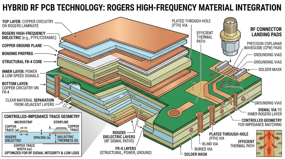
| High-Frequency PTFE | Rogers, Taconic, Arlon, Isola Astra, and equivalents | Dk 2.2-10.2, Df 0.0009-0.004, hybrid stack-ups | 5G mmWave, automotive radar, satellite, RF/microwave |
| Heavy Copper PCB | High-resin FR-4 or polyimide, any substrate per BOM | 3–20 oz copper, mixed weights, 2–10 layers | EV charging, solar inverters, welding, UPS, planar transformers |
| High-CTI PCB | High-CTI FR-4 (CTI ≥ 600V) | High voltage isolation, safety-critical | Power supplies, mains-connected equipment |
| Halogen-Free PCB | Halogen-free FR-4, phosphorus/nitrogen retardant | Environmental compliance, low smoke | Consumer, automotive, EU market products |