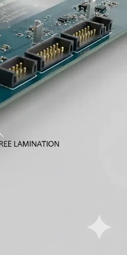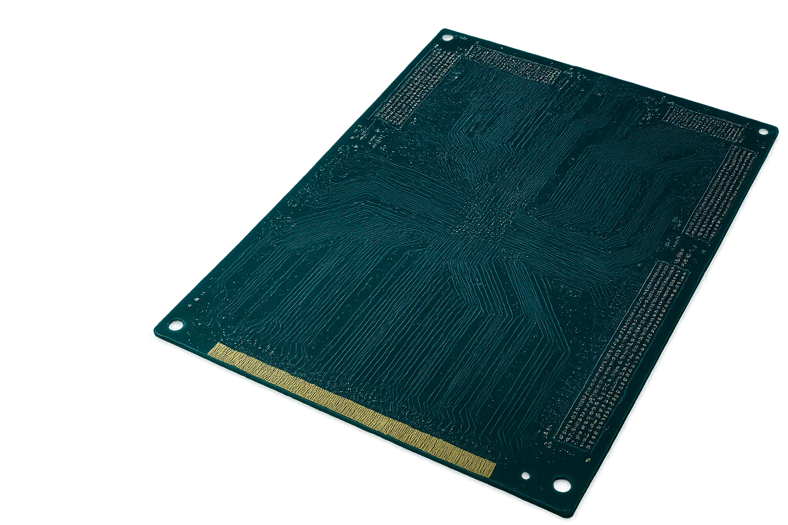
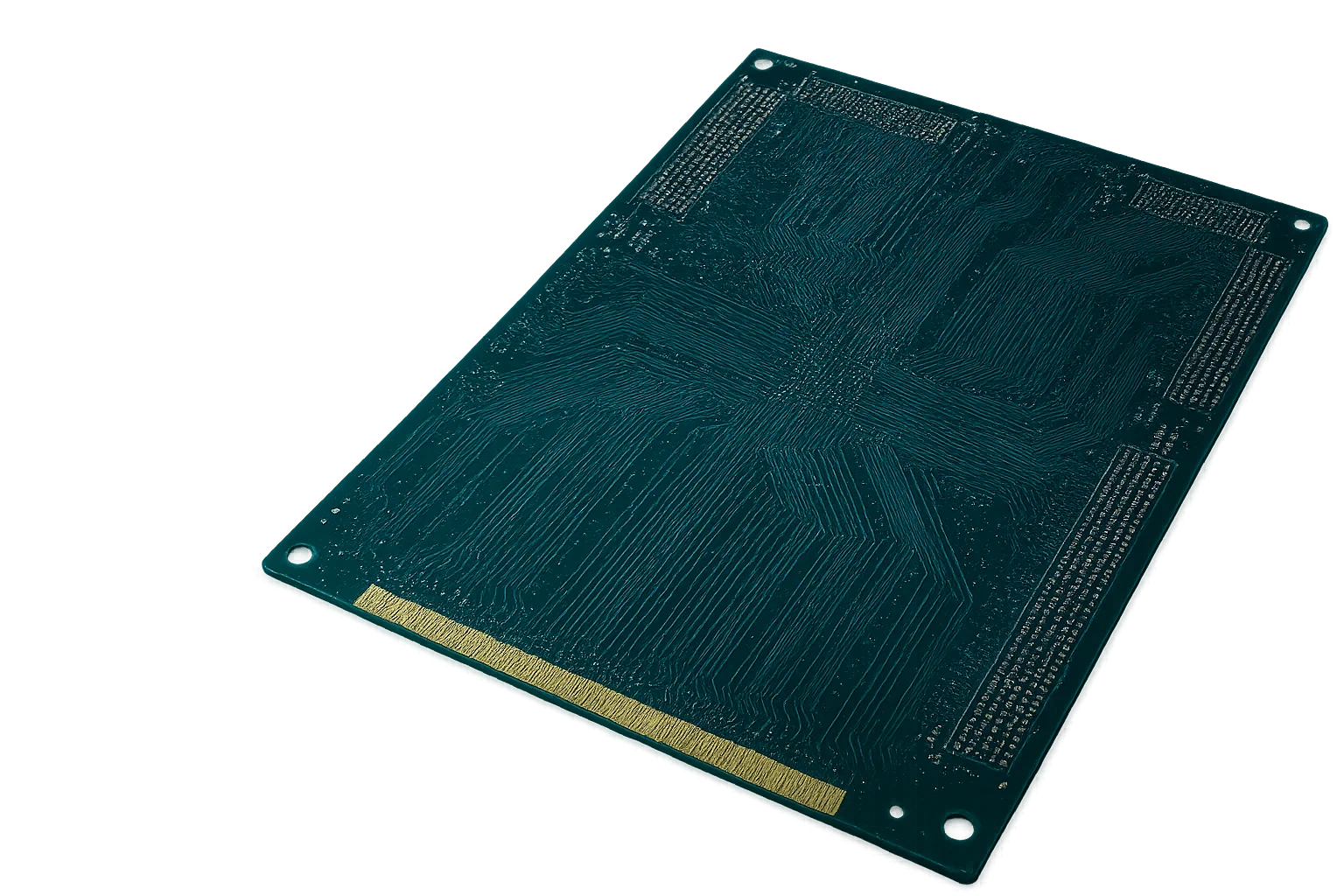
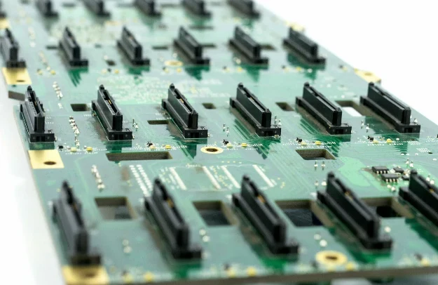
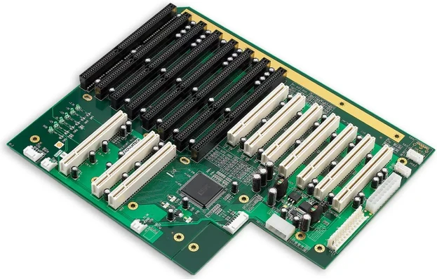
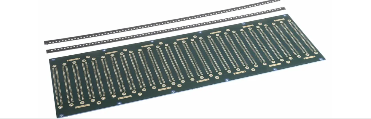
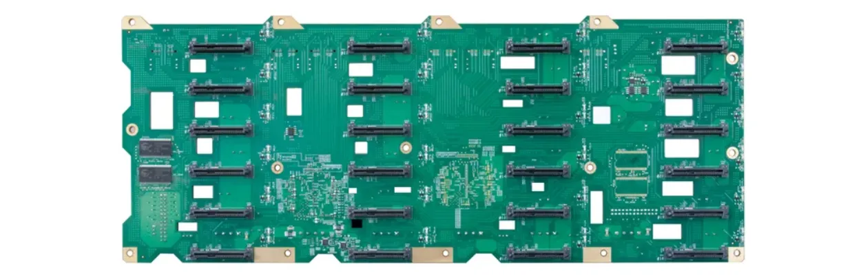
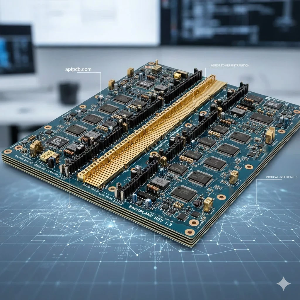
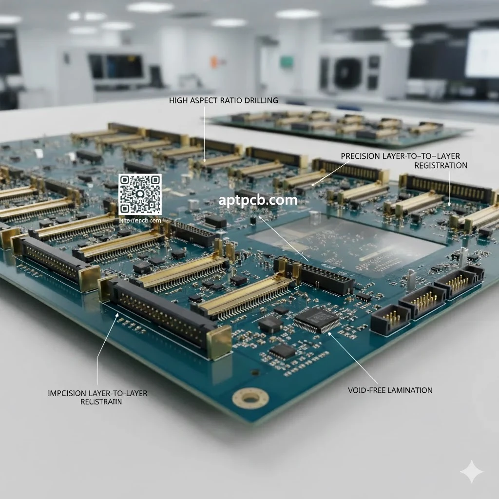
High-layer backplane PCB

LARGE FORMAT • 112G READY

Backplane PCB Manufacturing — High-Layer, Low-Loss, Press-Fit Ready

Extra-large backplanes up to 1100 × 500 mm with 24–50 layers, low-loss laminates, ±5% impedance, and CNC backdrill keep data center and telecom fabrics reliable at 112G.

  • 24–50 layer capacity
  • Low-loss laminates
  • Press-fit ready
  • CNC backdrill
  • ±5% impedance
  • 112G PAM4

Get an Instant Quote

Full Quote →
24–50Layer Count
1100×500 mmMax Panel
0.5 ns/cmChannel Delay
Df ≤0.0015Loss Tangent
3.4–7.0 mmBoard Thickness
20:1 drillsAspect Ratio
Depth ≥8 milBackdrill Control
±5%Impedance
112GPAM4 Ready
24–50Layer Count
1100×500 mmMax Panel
0.5 ns/cmChannel Delay
Df ≤0.0015Loss Tangent
3.4–7.0 mmBoard Thickness
20:1 drillsAspect Ratio
Depth ≥8 milBackdrill Control
±5%Impedance
112GPAM4 Ready

Backplane Fabrication & Assembly

APTPCB specializes in backplane PCB manufacturing for high-layer-count, high-speed interconnect systems where registration accuracy, impedance consistency, and mechanical stability are critical. We support large-format structures and complex stackups designed for predictable signal performance and dependable connector interfaces—helping customers build scalable backplane architectures for servers, telecom, and modular systems.

Backplane assembly and testing at APTPCB includes connector integration workflows, inspection, and validation aligned to system-level reliability. By managing fabrication and assembly as a unified deliverable, we help customers reduce integration risk, improve deployment stability, and maintain consistent performance across production runs.

Backplane manufacturing

Backplane Projects Delivered

Hyperscale data center, telecom, industrial automation, and aerospace backplanes built on our lines.

Data center switch fabrics

Data center switch fabrics

Telecom baseband backplanes

Telecom baseband backplanes

Aerospace radar chassis

Aerospace radar chassis

Industrial automation hubs

Industrial automation hubs

Automotive test racks

Automotive test racks

Compute backplanes

Compute backplanes

Carrier-Grade Reliability

All backplanes receive impedance coupons, backdrill logs, AOI/X-ray, Hi-Pot, and optional S-parameter testing to ensure compliance up to 112G.

Download Backplane Checklist
24–50 layers1100×500 mmLow-loss laminatesDual backdrillPress-fit ready112G PAM4

APTPCB Backplane Manufacturing Services

Dedicated engineering, low-loss materials, and large-panel processing for mission-critical backplanes.

Backplane Configurations

Data center, telecom, industrial, and aerospace backplanes with stripline routing and heavy copper.

  • Dual stripline fabrics
  • Hybrid FR-4/low-loss
  • Heavy copper power interconnects
  • Rigid-flex backplanes
  • Modular midplanes

Via & Transition Management

  • Long plated through-holes
  • Backdrilled stubs
  • Resin-filled via-in-pad
  • Copper coins for power
  • Press-fit tooling holes

Sample Backplane Stackups

  • 26-layer low-loss stripline backplane
  • 32-layer dual backdrill fabric
  • 24-layer hybrid power + control backplane

Material & Design Guidelines

Select low-loss laminates (Megtron, Tachyon, I-Speed) and copper thickness optimized for press-fit connectors.

  • Document Dk/Df per layer with acceptable alternates.
  • Specify plating thickness for press-fit zones.
  • Plan copper balance to prevent bow/twist on large panels.
  • Detail prepreg styles and resin content for multi-lamination.

Reliability & Validation

Backplanes undergo impedance testing, IR/s-parameter correlation, AOI, X-ray, and Hi-Pot up to 4 kV to satisfy telecom and aerospace specs.

Cost & Application Guidance

  • Reuse qualified stackups for different chassis.
  • Panelize multiple midplanes per sheet.
  • Group backdrill depths to reduce machining time.

Backplane PCB Manufacturing Flow

1

Stackup & SI Review

Align loss budgets, conductor roughness, and reference planes.

2

Core Prep & Imaging

Large-format imaging for long traces.

3

Sequential Lamination

Multiple cycles for high-layer builds.

4

Drilling & Backdrill

Deep drilling plus CNC backdrill with verification.

5

Surface Finish & Mask

ENIG/ENEPIG + color-coded masks for assembly.

6

Testing & Validation

Impedance, electrical, Hi-Pot, and reliability tests archived.

Backplane Stackup Engineering

CAM + SI teams create stackups, impedance tables, and drill/backdrill files.

  • Confirm low-loss laminates and copper weights.
  • Define backdrill layers and depths.
  • Plan press-fit footprints and tolerances.
  • Model impedance and create coupon layouts.
  • Specify finish/coating keep-outs for connectors.
  • Document panelization, fiducials, and handling.
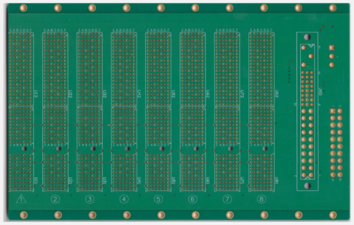
Manufacturing Execution

SPC on lamination, drilling, plating, and press-fit zones with feedback loops.

  • Monitor lamination pressure/temperature.
  • Measure drill diameter and plating thickness.
  • Verify backdrill depth and record logs.
  • Perform AOI/X-ray and impedance testing.
  • Run Hi-Pot and optional S-parameter tests.
  • Package large panels with bracing and desiccant.

Advantages of Backplane PCBs

High signal integrity, large format, and robust power delivery.

High Layer Density

24–50 layers with dedicated signal/power groups.

High-Speed Ready

Low-loss laminates and backdrill for 112G links.

Press-Fit Compatibility

Tight hole tolerances and plating.

Reliability Data

Comprehensive SI + electrical testing.

System Simplification

Reduces harness complexity and rework.

Documentation

Stackup, drill, and test packages provided.

Large-Panel Manufacturing

Processes panels up to 1100 × 500 mm with controlled flatness for chassis backplanes.

Embedded SI Team

CAM + SI engineers co-own backdrill tuning, launch optimization, and compliance reports.

Why Choose APTPCB?

Integrated backplanes simplify wiring, improve reliability, and scale to hyperscale bandwidth needs.

APTPCB production line
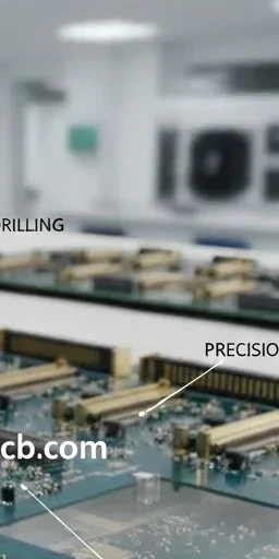
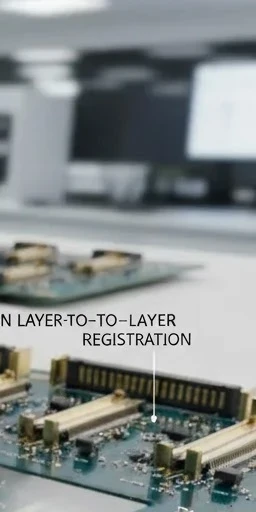
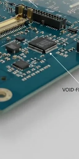
Large-format drilling • Backdrill verification • Press-fit testing

Backplane PCB Applications

Hyperscale networking, telecom infrastructure, industrial automation, and aerospace systems rely on high-layer backplanes.

Large-format processing and low-loss materials keep links stable at scale.

Telecom & Network

Telecom & Network

Switches, routers, and base stations.

SwitchRouterBaseband
Data Center & AI

Data Center & AI

Leaf-spine fabrics and accelerator backplanes.

Leaf-spineAI
Aerospace & Defense

Aerospace & Defense

Mission computers, radar, and avionics racks.

AvionicsRadar
Industrial Automation

Industrial Automation

Factory control and power distribution chassis.

Factory controlPower
Automotive & EV

Automotive & EV

Test benches and charging infrastructure.

Test rackCharger
Test & Measurement

Test & Measurement

ATE interfaces and load banks.

ATELoad bank
Medical & Imaging

Medical & Imaging

High-channel-count imaging systems.

ImagingDiagnostics
Rigid-Flex Backplanes

Rigid-Flex Backplanes

Folded harness replacements for compact enclosures.

Rigid-flexCompact systems

Backplane Design Challenges & Solutions

Control loss, backdrill, impedance, and warpage on massive boards.

Common Design Challenges

01

Insertion Loss Budgets

Low-loss materials and copper roughness must align with 112G budgets.

02

Backdrill Planning

Multiple depths need clear documentation and verification.

03

Warpage Control

Large panels warp without copper balancing.

04

Press-Fit Integrity

Tight hole tolerances and plating thickness are critical.

05

Documentation Load

Customers require detailed stackup, drill, and test data.

06

Handling & Packaging

Large boards must ship flat without damage.

Our Engineering Solutions

01

Loss Modeling

Stackup + SI models keep insertion loss on target.

02

Backdrill Playbooks

We create drill tables, tolerances, and verification steps.

03

Copper Balance & Panel Design

Thieving and cross-hatching control warpage.

04

Press-Fit Guidelines

Hole size, plating, and finish rules documented.

05

Packaging Kits

Custom crates and supports ship large panels safely.

How to Control Backplane PCB Cost

Low-loss materials, backdrill, and large panels add cost—apply premium features only where needed. Reuse stackups, drill sets, and panel sizes across chassis to minimize NRE. Provide insertion loss, connector types, and panel constraints so we can scope the leanest solution.

01 / 08

Standardized Stackups

Use common high-layer stackups across product lines.

02 / 08

Testing Scope

Run full SI testing for qualification, sampling for production.

03 / 08

DFx Collaboration

Early review avoids over-spec’d copper or via rules.

04 / 08

Panel Utilization

Optimize outlines and fiducials for maximum yield.

05 / 08

Finish Alignment

Select ENIG/OSP combos depending on assembly needs.

06 / 08

Shared Tooling

Reuse drill hits and lamination tooling to reduce NRE.

07 / 08

Backdrill Grouping

Combine similar depths to cut machine time.

08 / 08

Material Forecasting

Reserve low-loss laminate lots for ongoing programs.

Certifications & Standards

Quality, environmental, and industry credentials supporting reliable manufacturing.

Certification
ISO 9001:2015

Quality management across sequential lamination and drilling.

Certification
ISO 14001:2015

Environmental controls for copper plating and prepreg handling.

Certification
ISO 13485:2016

Traceable documentation for regulated industrial and medical systems.

Certification
IATF 16949

Automotive-grade SPC, PPAP, and CAPA coverage.

Certification
AS9100

Aerospace process governance for mission-critical backplanes.

Certification
IPC-6012 / 6013

Class 3 acceptance for rigid and rigid-flex structures.

Certification
UL 796 / UL94 V-0

Safety and flammability compliance for global deployments.

Certification
RoHS / REACH

Hazardous substance controls for export shipments.

Selecting a Backplane Manufacturing Partner

  • Large panel processing up to 1100×500 mm.
  • Low-loss materials and SI engineering.
  • Backdrill, impedance, and S-parameter testing.
  • Press-fit assembly support.
  • Class 3 inspection and documentation.
  • 24-hour DFx feedback.
Engineers inspecting backplanes

Backplane PCB Quality & Cost Console

Backplane PCB Process & Economic Controls

Quality gates synced with the cost levers for high-layer backplanes and press-fit connectors.

Process & Reliability

Pre-Production Controls

Stack-Up Validation

  • Panel utilization+5–8%
  • Stack-up simulation±2% thickness
  • Material prep110 °C vacuum
  • DFM releasePer lot

Backplane PCB Launch Checks

• Model stack-ups around high-layer backplanes and press-fit connectors.

• Rotate outlines, mirror tails, and share coupons across programs.

• Record bake, moisture, and lamination setpoints per lot.

Registration

Registration & Imaging

Metrology

  • Layer registration±0.05 mm
  • Drill accuracy±15 μm
  • Fiducial captureSPC logged
  • AOI overlayPer panel

Metrology Feedback

• Calibrate drill/imaging offsets for Backplane PCB geometries.

• Capture coverlay/tooling alignment within ±0.05 mm.

• Push AOI & SPC overlays back to CAM for continuous tuning.

Testing

Electrical & Reliability

Reliability

  • Impedance & TDR±5% tolerance
  • Insertion lossLow-loss verified
  • Thermal cycling> 100 cycles
  • DocumentationLot traceability

Reliability Evidence

• Match impedance, loss, or thermal coupons to high-layer backplanes and press-fit connectors nets.

• Log stress, CAF, or thermal results with each shipment.

• Archive micro-sections, X-ray, and electrical data for traceability.

Integration

Assembly Interfaces

Integration

  • Cleanroom SMTCarrier ready
  • Moisture control≤ 0.1% RH
  • Coating masksVersioned
  • ECN flowClosed loop

Assembly Controls

• Publish SMT carriers and handling rules for Backplane PCB assemblies.

• Define moisture exposure windows and nitrogen bake requirements.

• Sync ECNs with coating, stiffener, or hardware revisions.

Architecture

Stack-Up Economics

Architecture

  • Lamination cyclesOptimize 1+N+1/2+N+2
  • Material mixHybrid when needed
  • Copper weights0.5/1 oz mix
  • BOM alignmentPreferred cores

Stack-Up Strategy

• Pick stack-ups that balance thick stack-ups and lamination cycles demands.

• Standardize dielectric & copper sets per platform family.

• Apply premium laminates only where performance dictates.

Interconnect

Routing & Via Strategy

Interconnect

  • Via strategyStaggered priority
  • Backdrill planShared depths
  • Buried reuseMulti-net
  • VIP / tent usageAs required

Interconnect Controls

• Favor staggered/buried vias to avoid unnecessary fill cycles.

• Share drill maps, backdrills, and routing templates across builds.

• Limit via-in-pad or resin fill to fine-pitch or RF zones.

Utilization

Panel Efficiency

Utilization

  • Outline rotation+4–6% yield
  • Coupon sharingMulti-program
  • Tooling reusePanel families
  • Depanel strategyStandard tabs

Panel Optimization

• Rotate outlines and gang coupons to reclaim panel area.

• Re-use depanel tabs, fiducials, and tooling per family.

• Coordinate coupon placement for faster AOI and test.

Execution

Supply Chain & Finish

Execution

  • Material poolingMonthly ladder
  • Dual-sourcePPAP ready
  • Finish mixENIG / OSP
  • Logistics lanes48 h consolidation

Supply Levers

• Pool laminates, copper, and specialty films on a monthly cadence.

• Maintain dual-source approvals for critical materials.

• Align logistics lanes and 48 h consolidation windows per region.

Backplane PCB FAQ

Questions on panel size, materials, and validation.

Backplane PCB Manufacturing — Upload Data for SI Review

Large-format Class 3 lines
24–50 layer capability
Low-loss & backdrill expertise
Comprehensive SI documentation

Send stackups, panel drawings, and connector maps—our team replies with DFx notes, SI plans, and schedules within one business day.