Advanced Engineering Guide
The Engineering Reality of High-Layer-Count PCB Manufacturing
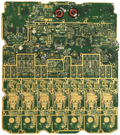
Designing a 32-layer backplane or a 24-layer AI motherboard in ECAD software is a complex routing puzzle, but manufacturing it is a battle against physics, chemistry, and thermodynamics. As layer counts increase, the margin for error shrinks exponentially. At APTPCB, we partner with senior hardware engineers globally to transition these extreme designs from the digital realm to physical reality. Below is a deep dive into the engineering hurdles of high-layer-count fabrication and how we solve them.
1. The Tyranny of Registration and Dimensional Scaling
The single greatest threat to a high-layer-count board is registration failure. A PCB is built by pressing alternating layers of fully cured cores and uncured prepreg under extreme heat and hydraulic pressure (lamination). During this process, the materials expand, and as the resin cures and cools, they shrink. This dimensional scaling is anisotropic - it shrinks differently in the X (warp) and Y (weft) directions of the glass weave.
In a 4-layer board, a slight shift is easily absorbed by the annular ring, the copper pad surrounding a drilled hole. In a 40-layer board, if the inner layers shift inconsistently, a mechanical drill bit descending through the board will inevitably break outside the copper pad on layer 25, severing the connection or causing a fatal short to a nearby ground plane.
The APTPCB solution: our CAM engineers apply non-linear scaling factors to the artwork of every single layer, mathematically predicting the shrink rate based on that specific layer's copper density. During layup, we use X-ray induction bonding systems to physically align the inner layers relative to each other before the press cycle, guaranteeing layer-to-layer registration accuracy of ±1.5 mils.
2. High Aspect Ratio Plating: The Capillary Challenge
As layer counts increase, the board gets thicker. A 32-layer board can easily reach 5.0 mm (200 mils) in thickness. If you need to drill a 10 mil (0.25 mm) via through that board, you create a microscopic capillary tube with an Aspect Ratio of 20:1.
Standard DC electroplating systems rely on fluid dynamics to circulate copper-rich chemical baths through the holes. In a 20:1 via, the fluid at the center of the barrel stagnates. The copper ions are depleted, and the plating process stops, resulting in a via with thick copper at the surface but dangerously thin (or completely missing) copper in the middle. During the extreme heat of SMT reflow or wave soldering, the Z-axis expansion of the board will easily tear this thin copper barrel apart, causing intermittent open circuits that are notoriously difficult to debug.
The APTPCB Solution: For boards exceeding a 10:1 aspect ratio, we deploy Periodic Reverse Pulse Plating. Instead of a continuous direct current, the system rapidly pulses the current forward, then briefly reverses it. The reverse pulse acts like an electrical "pump," stripping away depleted chemicals and pulling fresh, copper-rich fluid deep into the center of the via. This guarantees a uniform, thick copper barrel wall that survives multiple lead-free reflow cycles.
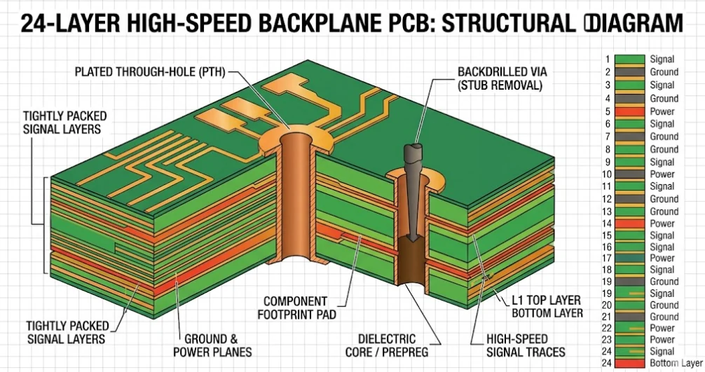
3. Defeating Signal Resonance with Precision Backdrilling
In high-speed digital architectures (PCIe Gen5, 100G/400G Ethernet, 112G PAM4), the physical geometry of the via becomes an active RF component. Imagine a signal traveling from Layer 1 down to Layer 5 on a 24-layer backplane. The signal successfully exits at Layer 5, but the remaining copper via barrel—continuing from Layer 6 all the way down to Layer 24—acts as an unterminated antenna (a "via stub"). This stub reflects electromagnetic energy back into the channel, causing destructive interference and closing the data eye diagram.
The APTPCB Solution: To rescue signal integrity, we utilize Controlled-Depth Backdrilling. Using advanced CNC drilling machines equipped with conductive surface-sensing technology, the drill bit enters from the bottom of the board (Layer 24) and drills out the unwanted copper stub, stopping precisely before it hits the active signal layer (Layer 5). We routinely achieve depth accuracies of ±50μm, leaving a harmless residual stub of less than 8-10 mils, thereby clearing the channel of destructive resonances.
4. Managing Impedance in Thick Architectures
In a 6-layer board, a 50Ω single-ended trace might require a 6-mil width. In a 32-layer board, because you must use ultra-thin prepregs (e.g., 2 mils thick) to keep the total board thickness manageable, the distance between the signal trace and its reference ground plane is drastically reduced. To maintain that same 50Ω impedance, the trace width must shrink proportionally, often down to 2.5 or 3 mils.
Etching a 3-mil trace with ±5% impedance tolerance requires absolute chemical mastery. The APTPCB Solution: We utilize Laser Direct Imaging (LDI) for sub-mil exposure accuracy, paired with vacuum-assisted etching lines that pull acid out from between the tight traces to prevent undercutting. We model every impedance structure in Polar Si9000 and physically verify the output using TDR (Time-Domain Reflectometry) test coupons on every single production panel.