4–20 OZ PROGRAMS

Heavy Copper PCB Manufacturing — Power Density Without Compromise

Build 4–20 oz copper power boards with embedded bus bars, selective thick plating, and thermal vias engineered for converters, EV powertrains, and industrial drives.

  • 4–20 oz outer copper
  • Embedded bus bars
  • Selective thick plating
  • Thermal via arrays
  • Press-fit/bolted hardware
  • IPC Class 3 reliability

Get an Instant Quote

Full Quote →

Heavy Copper Fabrication & Assembly

APTPCB engineers review current requirements, copper balance, and thermal paths before tooling, locking stackups that combine 4–20 oz copper with controlled resin flow.

We plan selective plating, embedded copper bars, and press-fit zones so high-current nets remain planar while signal layers stay manufacturable.

Assembly teams prepare fixtures, torque specs, and potting guidance for high-mass boards, delivering power modules ready for bus bars, studs, or heatsinks.

Heavy Copper Fabrication & Assembly

Heavy Copper Programs Delivered

Representative converters, EV systems, industrial drives, and defense power modules built in our lines.

EV traction inverters

EV traction inverters

Battery management backplanes

Battery management backplanes

Industrial motor drives

Industrial motor drives

Power supplies & rectifiers

Power supplies & rectifiers

Defense power distribution

Defense power distribution

Renewable energy converters

Renewable energy converters

Power Density with Verified Reliability

Thick copper plating, planarization, and Class 3 inspection ensure high-current boards survive thermal shock and vibration.

Download Capabilities
4–20 oz copperSelective platingThermal viasEmbedded bus barsHeatsink integrationPress-fit hardware

APTPCB Heavy Copper Manufacturing Services

Design-to-build support covering stackups, copper distribution, plating, and assembly for high-current electronics.

Heavy Copper PCB Types

Single-sided power planes, double-sided converters, multilayer control + power hybrids, and metal-backed modules.

  • Single-Sided Heavy Copper – 4–12 oz outer copper for bus bars and power planes.
  • Double-Sided Power – Symmetric 6–10 oz copper for converters and power supplies.
  • Multilayer Hybrid – Heavy copper outer layers with control inner layers.
  • Metal Core / IMS – Aluminum or copper cores bonded to heavy copper traces.
  • Embedded Bus Bar – Copper bars or coins buried inside dielectric for ultra-high current.

Via & Thermal Structures

  • Thermal Via Arrays: Dense plated vias transfer heat into heatsinks or housings.
  • VIPPO: Via-in-pad plated over to tie components directly to thick copper planes.
  • Backdrilled Power Vias: Remove stubs to reduce inductance on high-current nets.
  • Embedded Copper Coins: Replace thermal vias around hotspots.
  • Press-fit Vias: Plated holes sized for studs or terminals.

Sample Heavy Copper Stackups

  • 6 mm Single-Sided: 10 oz copper on FR-4 for bus bar replacement.
  • 8-Layer Hybrid: 6 oz outer copper, 2 oz inner signal layers, heavy thermal vias.
  • Metal-Core Power Module: 4 oz copper on aluminum IMS with plated cavities.

Material & Design Guidelines

Balance heavy copper with high-Tg laminates, resin-coated foils, and controlled prepreg flow to prevent delamination.

  • Use high-Tg, high-CTI laminates to handle heat and current.
  • Balance copper distribution per layer to prevent bow/twist.
  • Plan resin dams and thieving to control plating thickness.
  • Specify minimum land widths and spacing for thick copper etch.

Reliability & Validation

Heavy copper boards undergo cross-section analysis, thermal shock, and high-current cycling to validate performance before shipment.

Cost & Application Guidance

  • Selective plating: Apply 10–20 oz only where needed, keep signal layers lighter.
  • Shared tooling: Reuse proven panel sizes and drill sets to cut lead time.
  • Co-design bus bars: Integrate copper bars early to avoid rework.

Heavy Copper PCB Manufacturing Flow

1

Stackup & Current Modeling

Align copper thickness, dielectric, and thermal paths with current targets.

2

Imaging & Etch Prep

Adjust trace compensation for thick copper geometries.

3

Plating & Copper Build-Up

Sequential plating, planarization, and inspection to achieve target thickness.

4

Mechanical Ops

Route cavities, drill press-fit holes, prep heatsink or bus bar interfaces.

5

Assembly Readiness

Clean, tin, or finish surfaces; prep carriers and torque fixtures.

6

Validation & Test

High-current cycling, hipot, and thermal imaging with documentation.

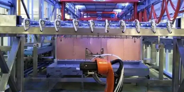
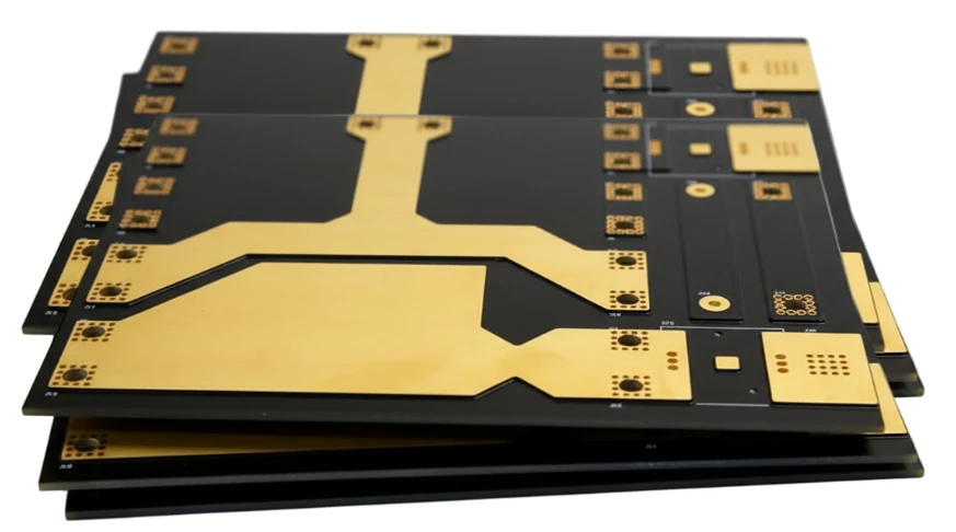
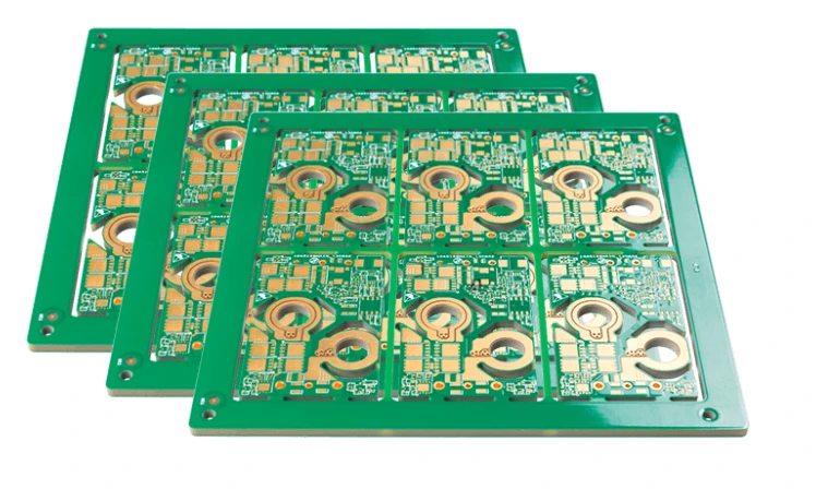
Heavy Copper CAM & Stackup Engineering

CAM teams map copper balance, plating schedule, and thermal via patterns before manufacturing.

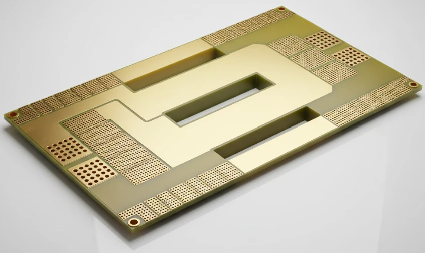
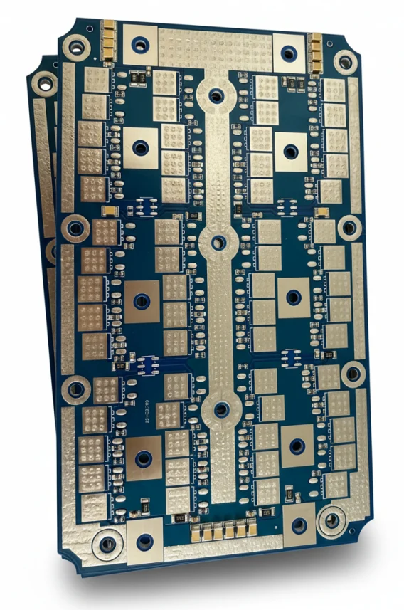
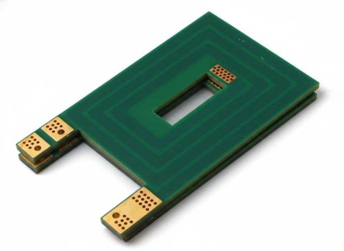
  • Confirm copper thickness per layer and plating sequence.
  • Define thieving, resin dams, and relief patterns to manage plating.
  • Plan thermal via arrays and copper coins where needed.
  • Document drill/press-fit tolerances and torque specs.
  • Specify surface finish (ENIG, tin, silver) for high-current pads.
  • Provide assembly notes for heatsinks, studs, or potting.
  • Release packaging requirements for heavy panels.

Manufacturing Execution & Feedback

Process engineers monitor plating thickness, lamination pressure, and post-plate planarity, feeding data back to design.

  • Track plating thickness with inline measurements.
  • Inspect for voids, delamination, or resin starvation after lamination.
  • Verify planarization before soldermask or finish.
  • Check press-fit hole size and cleanliness.
  • Run electrical, hipot, and thermal cycling tests.
  • Package boards with supports to avoid warpage or damage.
4–20 oz

Copper Thickness

Outer layers

2–10 oz

Inner Copper

Hybrid control + power

Class 3

Quality Level

IPC-6012 compliant

200 A+

Current Capability

Depending on width & cooling

Advantages of Heavy Copper PCBs

Deliver higher current, better thermal paths, and lower system cost.

High Current Density

4–20 oz copper handles hundreds of amps without overheating.

Mechanical Robustness

Thicker copper and high-Tg laminates resist thermal shock.

Thermal Management

Thermal vias, coins, and IMS cores move heat efficiently.

Compact System Design

Combine power + control layers into one assembly.

Lower Wiring Cost

Eliminate external bus bars and harnesses.

Reliability Documentation

Cross-sections, plating logs, and thermal tests included.

Why Choose APTPCB?

Integrated heavy copper planes reduce wiring, support higher temperatures, and simplify assembly.

EV powerIndustrial drivesRenewablesDefense powerRailwayUPS
APTPCB production line
Heavy copper plating line

Heavy Copper PCB Applications

High-current, high-reliability systems across transportation, energy, and industry.

Integrated heavy copper PCBs replace bus bars and improve thermal performance.

EV & Transportation

Inverters, battery management, and onboard chargers.

Traction inverterOBCBMSDC-DCCharging

Industrial Drives

Motor drives, robotics, and factory power systems.

Motor driveRoboticsAutomationUPSPower supply

Energy & Storage

Solar combiner boxes, wind converters, and ESS modules.

SolarWindESSMicrogridHVDC

Defense & Aerospace Power

Rugged power distribution and radar supply modules.

Radar PSUActuationRad-hardAvionics

Heavy Equipment

Mining, rail, and industrial equipment controllers.

RailMiningCranesHVAC

Power Electronics OEMs

High-density power supply and UPS manufacturers.

PSUUPSServer powerDatacenter

Bus Bar Replacement

Custom copper coin/bus bar integration for compact systems.

Bus barCopper coinCompact power

Test & Validation

Load banks, power test fixtures, and labs.

Load bankPower testLab equipment

Heavy Copper Design Challenges & Solutions

Balancing copper thickness, manufacturability, and thermal management requires early coordination.

Common Design Challenges

01

Copper Balance

Uneven copper thickness causes bow/twist and lamination defects.

02

Etch Definition

Thick copper traces need compensation to hold width and spacing.

03

Thermal Stress

High current generates heat that must be dissipated to avoid delamination.

04

Press-fit Integrity

Hole wall quality and plating thickness dictate connector reliability.

05

Surface Finish Selection

Finish must handle high current without increasing resistance.

06

Assembly Handling

Heavy panels need fixtures and support to avoid damage.

Our Engineering Solutions

01

Copper Balancing & Thieving

We add copper pours and thieving to keep plating uniform.

02

Advanced Etch Compensation

CAM applies compensation curves tuned for thick copper.

03

Thermal Modeling Support

DFx reviews align thermal vias, coins, and heatsinks.

04

Press-fit & Hardware Guides

Hole tolerances, plating specs, and torque data are documented.

05

Finish Optimization

Recommend ENIG, tin, or silver based on current and assembly method.

How to Control Heavy Copper PCB Cost

Most cost is driven by plating cycles, copper usage, and machining—reserve the heaviest copper for true high-current paths. Designing with standard panel sizes, drill sets, and finishes keeps lead time and pricing predictable. Share current density maps, thermal expectations, and hardware requirements early to align stackups and tooling.

01 / 08

Selective Copper Zones

Use step plating or coins to thicken only critical areas.

02 / 08

Align Finish to Need

ENIG or immersion silver suits most; reserve tin/silver plating for solder-lug areas.

03 / 08

Material Planning

Lock laminate and copper buys for multi-build programs.

04 / 08

Optimize Panel Utilization

Rotate outlines and share tooling across part numbers.

05 / 08

Consolidate Hardware

Use shared studs or terminal patterns to reduce machining.

06 / 08

Collaborative DFx

Early stackup and plating reviews prevent respins.

07 / 08

Standardize Drill Sizes

Align press-fit and via diameters with stocked tooling.

08 / 08

Plan Assembly Fixtures

Reusable carriers lower setup time for heavy panels.

Certifications & Standards

Quality, environmental, and industry credentials supporting reliable manufacturing.

Certification
ISO 9001

Quality Management

Certification
ISO 14001

Environmental Management

Certification
ISO 13485

Medical Devices

Certification
IATF 16949

Automotive Quality

Certification
AS9100

Aerospace Quality

Certification
IPC-6012

Rigid PCB Class 3

Certification
IPC-6013

Rigid-Flex & Flex

Certification
UL Recognized

94V-0 / Safety

Certification
RoHS / REACH

Material Compliance

Selecting a Heavy Copper Manufacturing Partner

  • 4–20 oz plating capability with SPC control.
  • Embedded coin/bus bar integration experience.
  • High-Tg laminate sourcing and traceability.
  • Press-fit, solder, and bolted hardware assembly support.
  • Thermal cycling, cross-section, and hipot testing in-house.
  • 24-hour DFx feedback with bilingual engineers.
Engineers reviewing heavy copper panels

Quality & Cost Console

Process & Reliability Controls + Economic Levers

Unified dashboard connecting HDI quality checkpoints with the economic levers that compress cost.

Process & Reliability

Pre-Lamination Controls

Stack-Up Validation

  • Panel utilization+5–8%
  • Stack-up simulation±2% thickness
  • VIPPO planningPer lot
  • Material bake110 °C vacuum

Pre-Lamination Strategy

• Rotate outlines, mirror flex tails

• Share coupons across programs

• Reclaim 5-8% panel area

Registration

Laser & Metrology

Registration

  • Laser drill accuracy±12 μm
  • Microvia aspect ratio≤ 1:1
  • Coverlay alignment±0.05 mm
  • AOI overlaySPC logged

Laser Metrology

• Online laser capture

• ±0.05 mm tolerance band

• Auto-logged to SPC

Testing

Electrical & Reliability

Testing

  • Impedance & TDR±5% tolerance
  • Insertion lossLow-loss verified
  • Skew testingDifferential pairs
  • Microvia reliability> 1000 cycles

Electrical Test

• TDR coupons per panel

• IPC-6013 Class 3

• Force-resistance drift logged

Integration

Assembly Interfaces

Integration

  • Cleanroom SMTCarrier + ESD
  • Moisture control≤ 0.1% RH
  • Selective materialsLCP / low Df only where needed
  • ECN governanceVersion-controlled

Assembly Controls

• Nitrogen reflow

• Inline plasma clean

• 48h logistics consolidation

Architecture

Stack-Up Economics

Architecture

  • Lamination cyclesOptimize 1+N+1/2+N+2
  • Hybrid materialsLow-loss where required
  • Copper weightsMix 0.5/1 oz strategically
  • BOM alignmentStandard cores first

Cost Strategy

• Balance cost vs performance

• Standardize on common cores

• Low-loss only on RF layers

Microvia Planning

Via Strategy

Microvia Planning

  • Staggered over stacked-18% cost
  • Backdrill sharingCommon depths
  • Buried via reuseAcross nets
  • Fill specificationOnly for VIPPO

Via Cost Savings

• Avoid stacked microvias

• Share backdrill tools

• Minimize fill costs

Utilization

Panel Efficiency

Utilization

  • Outline rotation+4–6% yield
  • Shared couponsMulti-program
  • Coupon placementEdge pooled
  • Tooling commonalityPanel families

Panel Optimization

• Rotate for nesting efficiency

• Share test coupons

• Standardize tooling

Execution

Supply Chain & Coating

Execution

  • Material poolingMonthly ladder
  • Dual-source PPAPPre-qualified
  • Selective finishENIG / OSP mix
  • Logistics lanes48 h consolidation

Supply Chain Levers

• Pool low-loss material

• Dual-source laminates

• Match finish to need

Heavy Copper PCB Manufacturing — Upload Data for Power Review

IPC Class 3 inspection
4–20 oz plating expertise
Embedded coin integration
Thermal & power validation

Send schematics, stackups, and current maps—we respond with DFx notes, plating flow, and build schedule within one business day.

Heavy Copper PCB FAQ

Key information about copper thickness, thermal management, and assembly.