Electrical Testing

Flying Probe Testing (FPT) for PCB & PCBA

High-reliability electronics start with high-reliability testing. APTPCB's Flying Probe Testing (FPT) platform delivers precise, fixture-free electrical verification for both bare PCBs and fully assembled PCBAsβ€”ensuring defects are identified early, accurately, and cost-effectively.

Get an Instant Quote

Software-DrivenZero Fixture Cost
Fine-Pitch AccessHigh Accuracy
Rapid PrototypingFast Setup
No Board ModsNon-Destructive

Flying Probe Testing: Precision Electrical Verification Without Fixtures

High-reliability electronics start with high-reliability testing. At APTPCB, our Flying Probe Testing (FPT) platform delivers precise, fixture-free electrical verification for both bare PCBs and fully assembled PCBAsβ€”ensuring defects are identified early, accurately, and cost-effectively.
Whether you are accelerating prototyping or optimizing small/medium-volume production, APTPCB's FPT provides the coverage, flexibility, and traceability needed for modern electronic products.

What Is Flying Probe Testingβ€”and Why It Matters

Flying Probe Testing (FPT) is a high-precision, non-fixture electrical test method that uses independently controlled probes to verify circuit connectivity, component integrity, and assembly quality.
Compared with traditional bed-of-nails fixtures, FPT offers:
  • Zero fixture cost – ideal for frequent design changes
  • High accuracy – probes access fine-pitch, densely populated areas
  • Fast program setup – crucial for prototypes and time-sensitive builds
  • Non-destructive verification – no special test pads or board modification required
During testing, robotic probes perform critical checks, including:
  • Continuity & open circuit verification
  • Short-circuit detection
  • Component value measurement (R / C / L)
  • Diode/transistor polarity & functionality
  • Power net and isolation testing
FPT ensures electrical integrity earlyβ€”reducing rework, improving yield, and supporting rapid, reliable product launches.

Maximize FPT Efficiency: Design Guidelines for Optimal Test Points

To ensure the most effective and efficient flying probe testing for your PCBAs, APTPCB's engineers work with you to implement best practices for test point design. Thoughtful design at this stage significantly enhances test coverage, speed, and accuracy, ultimately saving you time and cost.
1. Ensure Accessibility to All Critical Nets:
  • Strategic Placement – Distributing test points across the board to cover all necessary circuits
  • Obstruction Avoidance – Designing layouts that prevent components or other board features from blocking probe access
  • Dual-Side Coverage – Utilizing both top and bottom sides of the PCB for comprehensive test point placement
2. Optimize Test Point Features for Reliability:
  • Size – Test points should be optimally sized (typically 0.5mm to 1mm diameter)
  • Shape – Circular test points are standard, with flexibility for other shapes if needed
  • Surface Finish – A smooth, flat, and conductive surface finish (like ENIG or HASL) is crucial
  • Solder Mask Clearance – Adequate clearance around the test point prevents solder mask interference
  • Clear Labeling – Well-defined labeling facilitates easier test program development
3. Account for Secure Board Clamping:
  • Designated Clamping Areas – Identifying specific, non-critical regions on the PCB for clamping
  • Edge Clearance – Maintaining sufficient space from board edges to accommodate clamping mechanisms
  • Stability – Ensuring the clamping method provides stable, flex-free support
  • Dual-Side Compatibility – Designing clamping areas compatible with testing from both sides
4. Understand Board Dimensions for Tester Compatibility:
  • Maximum Board Size – Verifying your PCB fits within the working envelope of our flying probe testers
  • Minimum Board Size – For very small boards, we develop special fixturing or adapters
  • Thickness – Accounting for board thickness relative to probe travel distance
  • Warpage Minimization – Advising on design practices to reduce board warpage
5. Manage Maximum Component Height for Probe Clearance:
  • Probe Clearance – Ensuring ample space for probes to navigate between components
  • Strategic Tall Component Placement – Advising on placement to minimize interference with probe paths
  • Dual-Side Testing Considerations – Accounting for cumulative height of components on both sides
  • Optimized Probe Tip Selection – Utilizing a variety of probe tips for varying heights

How APTPCB Delivers Precision: Our Flying Probe Testing Process

At APTPCB, our Flying Probe Testing is a sophisticated, multi-step process engineered for maximum precision and comprehensive defect detection.
1. Expert FPT Test Program Creation:
  • Detailed Design Analysis – Our engineers meticulously study your PCB design data (Gerber, CAD)
  • Precise Test Point Mapping – We create an accurate digital map of all designated test points
  • Optimized Test Sequence Planning – We strategically determine the most efficient sequence of tests
  • Probe Movement Optimization – Our software plans the most efficient paths for probe movement
  • Rigorous Test Parameter Definition – We set precise voltage levels, current limits, and measurement thresholds
2. Seamless Program Upload and Verification:
  • Secure File Transfer – The test program files are securely transferred to the tester's control system
  • Rigorous Program Verification – Automated checks ensure the program's compatibility
  • Precise Calibration – Any necessary calibrations are performed to guarantee accuracy
  • Initial Test Run – A trial run is conducted to verify the program's functionality
3. Automated Electrical & Power Test Signal Application:
  • Secure Board Loading – Your PCBA is carefully loaded onto the test bed and securely clamped
  • Automated Probe Positioning – The flying probes move to their initial positions
  • Controlled Signal Application – Electrical signals are precisely applied to specific points
  • Accurate Measurements – The tester measures various electrical parameters with high precision
  • Real-time Data Analysis – Measured values are continuously compared against expected values
  • Immediate Fault Detection – Any discrepancies are flagged in real-time with precise location information
  • Comprehensive Results Logging – All test results are meticulously recorded for quality control and traceability

The APTPCB Advantage: 10 Benefits of Our Flying Probe Testing

Unparalleled Design Flexibility

Easily adapt to new board designs and revisions without the delay or cost of custom fixtures, perfect for agile development.
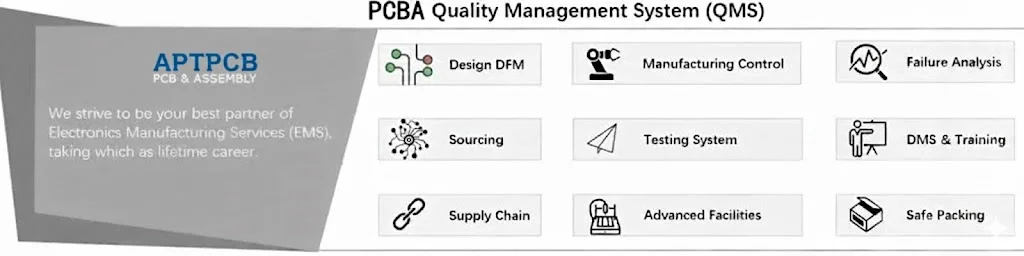
Superior Cost-Effectiveness

Eliminate expensive dedicated test fixtures for low to medium volume runs, leading to substantial savings on your testing budget.

Rapid Setup & Production Ramp-Up

Achieve faster test program development and implementation, significantly accelerating your time-to-market for new products.

Exceptional Testing Precision

Our high-accuracy flying probes ensure reliable access and testing of even the most high-density boards and fine-pitch components.

Comprehensive Electrical Verification

Conduct a wide array of tests, including continuity, short circuit detection, component value measurement, and basic functional checks.

Preservation of Board Integrity

Enjoy non-destructive testing that requires no additional test points or modifications to your original board design.

Agile Program Modification

Quickly adapt test programs to accommodate design changes or focus on specific areas of concern without delays.

Reduced Infrastructure Costs

Benefit from the elimination of custom test fixtures, saving money, valuable storage space, and simplifying inventory management.

Enhanced Fault Diagnosis

Leverage the precise nature of FPT for accurate identification and localization of faults, streamlining troubleshooting and repair.

Actionable Data for Continuous Improvement

Access detailed test results and analytical data to drive comprehensive quality control and ongoing manufacturing enhancements.

Clarifying Your Testing Strategy: PCB Flying Probe Test vs. PCBA Flying Probe Test

While both Bare PCB and PCBA flying probe tests utilize similar advanced technology, they serve distinct purposes at different stages of your product's journey. Understanding these differences is crucial for implementing a comprehensive and effective quality control strategy.
Bare PCB Flying Probe Test: Foundational Integrity
  • Primary Focus: Verifies the integrity of the PCB itself, including copper traces, vias, and pads
  • Timing: Conducted after PCB fabrication but before component assembly
  • Key Test Types: Continuity, short circuit detection, impedance testing, and high-voltage isolation testing
  • Accessibility: Generally offers full, unobstructed access to all test points on both sides
  • Speed: Typically faster due to fewer obstacles and test points
  • Faults Detected: Manufacturing defects within the bare PCB, such as open circuits, shorts, or incorrect impedance
PCBA Flying Probe Test: Comprehensive Assembly Verification
  • Primary Focus: Evaluates both the underlying PCB and all mounted components (presence, orientation, value)
  • Timing: Conducted after component assembly, often as a critical intermediate or final quality check
  • Key Test Types: All bare PCB tests, plus component presence, orientation, value verification, and basic functional testing
  • Accessibility: May have more limited access to some test points due to component placement
  • Speed: Generally slower than bare PCB testing due to more complex test sequences
  • Faults Detected: Bare PCB defects, component placement errors, faulty components, incorrect component values, and assembly issues
In many cases, APTPCB recommends implementing both types of testing at different stages of production. Bare PCB FPT catches defects before valuable components are added, saving significant costs. PCBA FPT provides a final, comprehensive quality check, ensuring your completed assembly meets all specified requirements.

Partner with APTPCB for Unrivaled Flying Probe Testing Excellence

Flying probe testing has solidified its position as an indispensable tool in the modern electronics manufacturing industry. Its unparalleled flexibility, precision, and cost-effectiveness make it exceptionally valuable for:
  • Accelerating prototyping cycles
  • Optimizing small to medium production runs
  • Ensuring the integrity of complex or densely populated boards
By partnering with APTPCB, you leverage our expertise in best practices for test point design, coupled with a deep understanding of both bare PCB and PCBA flying probe testing. This empowers you to:
  • Significantly improve your product quality and reliability
  • Reduce your time-to-market
  • Enhance your overall manufacturing efficiency and profitability
As electronic designs continue their trajectory toward increased complexity and miniaturization, the role of APTPCB's advanced flying probe testing services will only grow in significance. Our ability to adapt to new designs and technologies positions us as your key partner in the future of electronics quality assurance.

Get Started with Flying Probe Testing

Ready to elevate the quality and reliability of your PCBAs? Contact APTPCB today to discuss your specific flying probe testing requirements and discover how our cutting-edge services can benefit your next project.