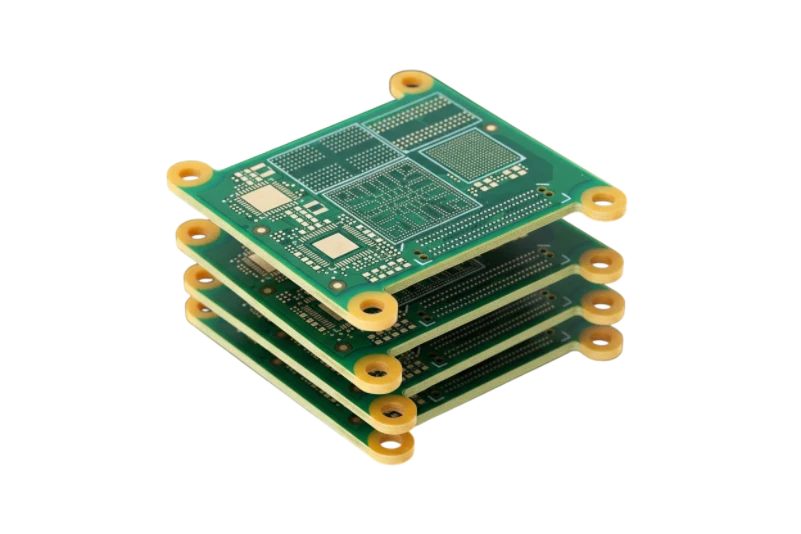
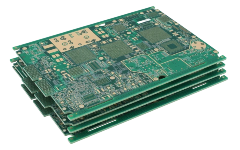
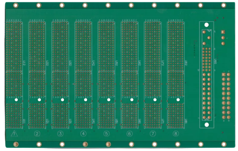
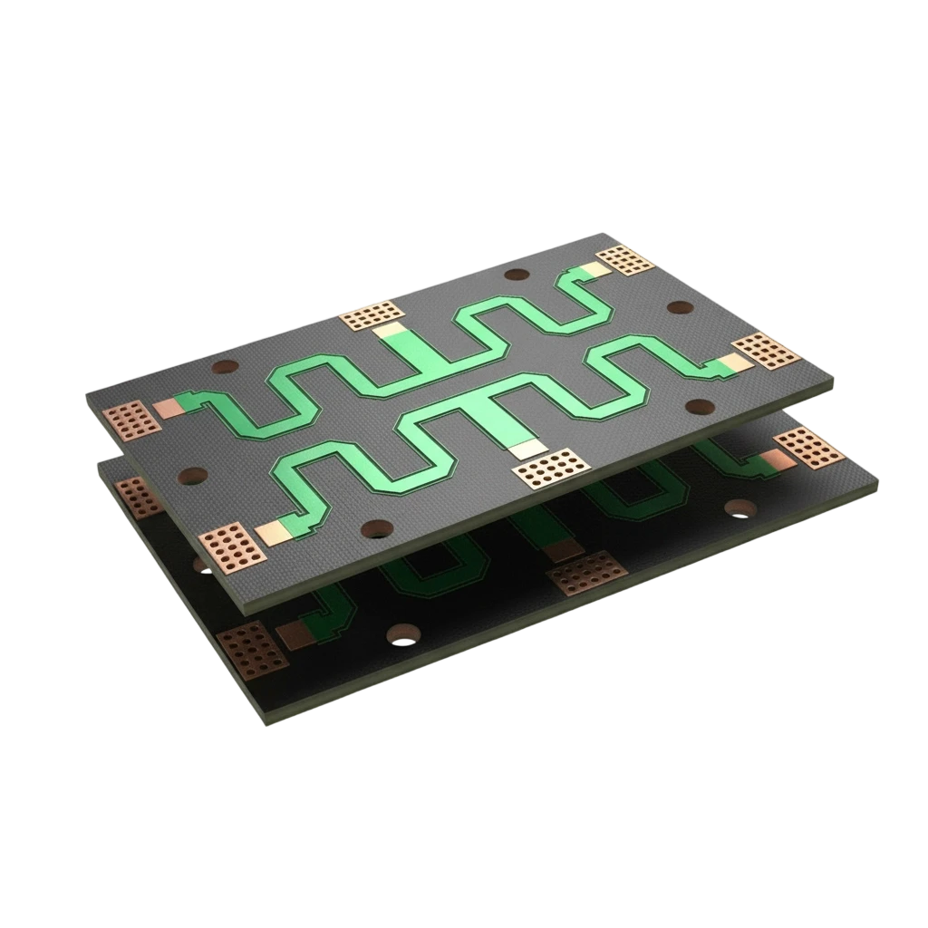
FR-4 PCB
MainstreamStandard FR-4 builds for cost-effective programs.
- Standard stackups
- Lead-free capable
- IPC class II/III
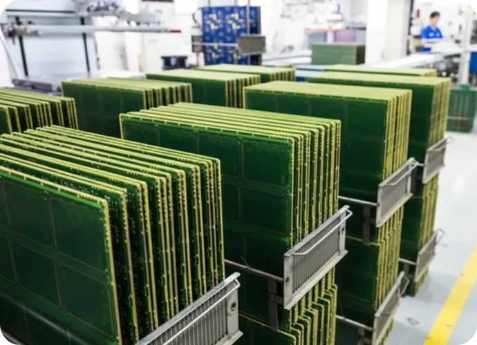
PCB Manufacturing
Stack-up strategy, impedance control, and yield optimization from prototype to mass production, covering HDI, RF, rigid-flex, and metal core designs, all manufactured to IPC standards for consistent quality.
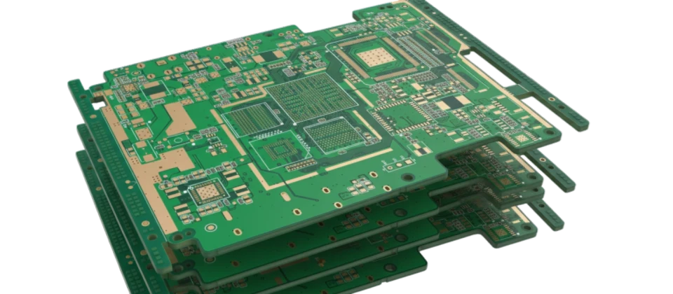
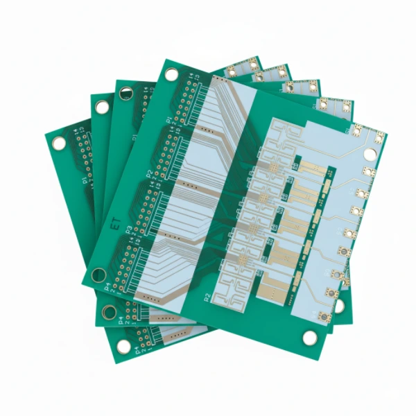
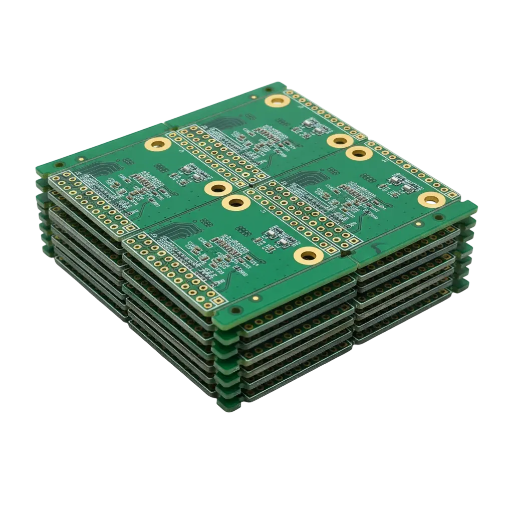
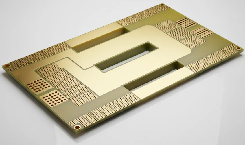
PCB Portfolio
Each product path is engineered with dedicated tooling, material strategy, and quality checkpoints to meet signal integrity, thermal, and reliability targets from prototypes to mass deployment.
Standard FR-4 builds for cost-effective programs.
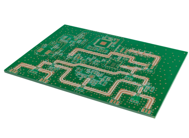
Low-loss, tight tolerance stackups for high-speed links.
Blind/buried vias, stacked uVias for dense layouts.
PTFE and hydrocarbon ceramics for RF paths.
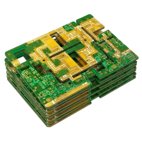
Deep layer counts with controlled impedance.
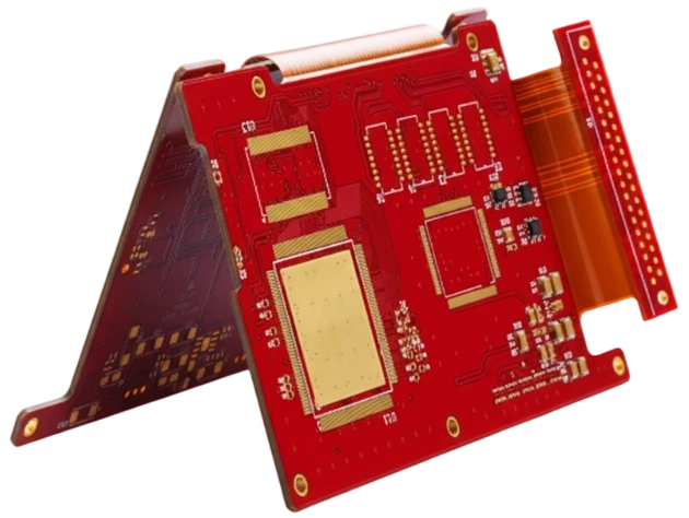
Hybrid rigid-flex for compact enclosures.
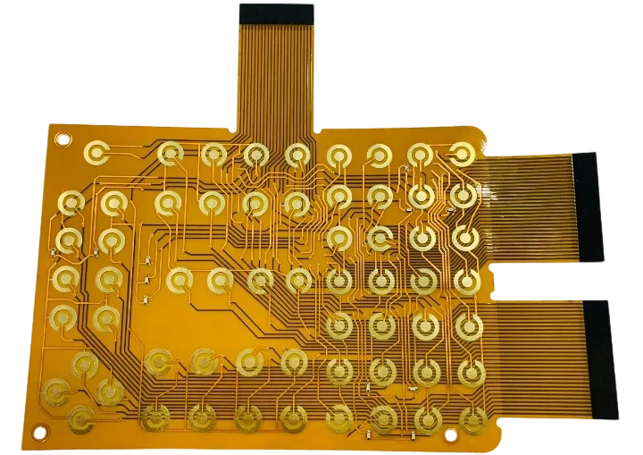
Single/dual-layer flex for interconnect and wearables.
Long-run, thick copper backplanes for telecom/datacom.
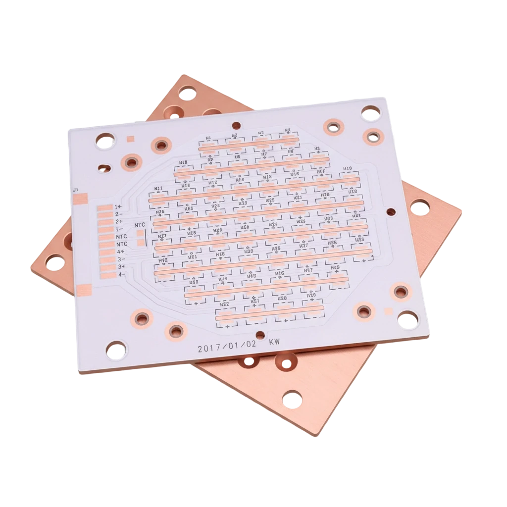
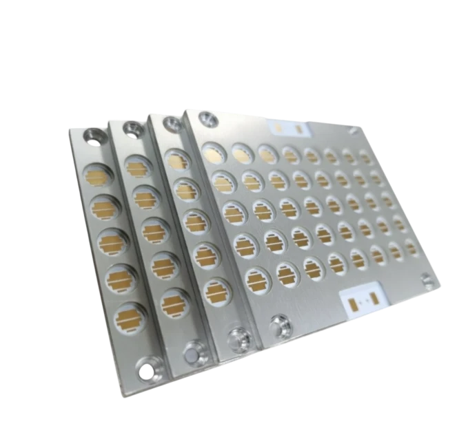
Aluminum / copper cores for thermal management.
Ceramic substrates for high temp / RF stability.
Higher Tg materials for thermal reliability.
Thick copper for high-current power designs.
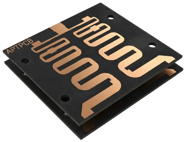
Custom antenna boards on RF laminates.
Low-loss materials for mmWave and high-speed.

TDR-verified impedance control for high-speed and RF designs.
Thermal vias, metals, and stackups for heat spread.
Engineering Toolkit
Validate stackups, inspect Gerbers, and run quick simulations without leaving the manufacturing workflow.
View Gerbers online for quick checks.
Launch ViewerInspect 3D PCB models in browser.
Open 3D ViewerSolve microstrip/stripline quickly.
Run CalculatorSimulate circuits online without install.
Open SimulatorProcess windows are matched to target stackups, copper distribution, and reliability requirements. Our MES and SPC systems surface trends before they impact production builds.
SPC-driven runs with monitored Cp/Cpk.
Approved vendors and lot-level traceability.
Coupon-driven impedance adjustments.
Documented press cycles and resin flows.
Customer programs span automotive ADAS controllers, industrial automation backplanes, telecom switching, and medical imaging modules. Typical results include <20 PPM field returns and 10–15 day ramp-to-mass-production.
12-layer HDI with blind/buried vias, ±5% impedance, PPAP documentation, <15 PPM over 18 months.
48-layer backplane with backdrill, Dk 3.5 hybrid stackups, BER <1e-12 at 25 Gbps post-install.
Share stackups, Gerbers, and impedance targets. Our CAM and SI teams respond within 24 hours with a manufacturability plan.
Answers to the questions we hear most from hardware teams preparing builds.