DFM/DFA Guidelines
Design for Manufacturing and Assembly best practices to optimize yield and quality.
- •Fabrication limits
- •Assembly rules
- •File submission
- •Quality standards
Resources
Everything linked in the Resources menu—knowledge packs, download centers, tools, and case studies—organized in one place.
Find the information you need, organized by topic for quick access to documentation and guides.
Design for Manufacturing and Assembly best practices to optimize yield and quality.
Material datasheets, process notes, and stackup PDFs mirrored from the resources menu.
Inspect files, validate BOMs, calculate impedance, and review designs in-browser.
A quick reference to common PCB manufacturing and assembly terms and abbreviations.
Technical articles, best practices, and practical engineering insights.
Quick answers to common questions about files, lead times, testing, and processes.
Design for Manufacturing and Assembly guidelines to improve yield, reduce costs, and accelerate production.
Inspect copper, drills, soldermask, and layers directly in the browser.
Review PCB files in a clean, browser-based viewer for fast collaboration.
Microstrip, stripline, and differential pair solver tied to the stackup lab.
Validate BOM metadata, alternates, and AVL notes before sourcing.
Quick browser-based circuit simulation for early validation and education.
Open a 3D preview of your PCB for quick mechanical checks and review.
Search common PCB manufacturing, assembly, and signal integrity terms.
Showing - of results.
Method of connecting circuits that blocks DC components while passing AC signals. Uses capacitors to isolate DC bias levels between stages.
Chemical compound in flux that removes oxides from metal surfaces to promote solder wetting during the soldering process.
PCB fabrication method where copper is selectively deposited onto a bare substrate, as opposed to subtractive etching.
Bond strength between copper and laminate substrate or between different PCB layers. Critical for reliability.
Circuit processing continuous signals, as opposed to digital circuits. Requires careful layout for noise immunity.
Copper area remaining around a drilled hole after fabrication. Measured from hole edge to pad edge. Minimum typically 4-6 mil.
Electrochemical process creating protective oxide layer on aluminum for heat sinks and chassis components.
Automated Optical Inspection. Machine vision system inspecting PCB assemblies for placement, polarity, solder quality, and missing parts.
Opening in solder paste stencil through which paste is deposited onto PCB pads. Size and shape critical for print quality.
Multiple PCBs arranged in a panel format for efficient manufacturing. Also called panelization or step-and-repeat.
Master pattern or digital files (Gerber) defining PCB layers including copper, solder mask, and silkscreen.
Ratio of PCB thickness to drilled hole diameter. Higher ratios (>10:1) require advanced plating processes.
Technical document showing component placement, orientation, polarity markings, and special assembly instructions.
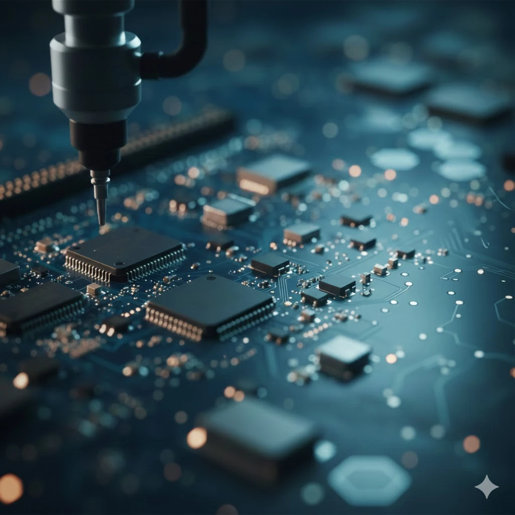
Assembly. Process of mounting and soldering electronic components onto a bare PCB to create a functional circuit board.
Automatic Test Equipment. Computerized testing systems for verifying PCB assembly functionality and performance.
Signal loss in a transmission line, measured in dB per unit length. Increases with frequency and trace length.
Approved Vendor List. Pre-approved component manufacturers and distributors meeting quality requirements.
American Wire Gauge. Standard for wire diameter measurement. Lower numbers indicate larger diameter.
Automated X-Ray Inspection. Non-destructive inspection using X-rays to examine hidden solder joints under BGAs and QFNs.
Solvent mixture maintaining constant composition during evaporation. Used in some cleaning processes.
Technical articles, best practices, and industry insights from our engineering team.
May 08, 2026 · Technology
A practical engineering guide to advanced PCB materials and substrates: how metal-core boards, flex structures, and package substrates change the manufacturing route, assembly route, and release boundary before first build.

May 08, 2026 · Technology
A practical engineering guide to high-speed and RF PCB manufacturing: how stackup direction, material scope, local transitions, shielding, and layered validation shape release readiness before pilot or mass production.

May 08, 2026 · Technology
A practical engineering guide to PCB cost reduction: how BOM clarity, stackup choices, HDI scope, surface finish, panel strategy, and DFM review affect quote complexity before RFQ.

May 08, 2026 · Technology
A practical engineering guide to PCB design for manufacturing: how release clarity, fabrication route, test strategy, and reliability evidence should be reviewed together before quote, pilot build, and volume release.

May 08, 2026 · Technology
A practical industry-solutions guide to PCB and PCBA programs: how medical, industrial control, advanced-interface, and power-electronics projects expose different board-level risks before quote and release.

May 08, 2026 · Technology
A practical engineering guide to quick-turn PCB prototypes: how lead time, DFM intake, factory routing, prototype validation, and shipping posture change compared with the standard release path.

Quick answers to common questions about our services and processes.
We accept Gerber files (RS-274X format preferred), ODB++, and Excellon drill files. For assembly, we need pick-and-place files (CSV/XLS), BOM, and assembly drawings (PDF). We also accept native CAD files from Altium, KiCad, Eagle, and OrCAD for conversion if needed.
Standard prototype lead time is 5-7 business days for PCB fabrication and an additional 3-5 days for assembly after component receipt. We offer expedited services with 24-48 hour quick-turn options for urgent requirements.
We have no minimum order quantity. We support everything from single prototype boards to high-volume production runs of millions of units. Our pricing scales based on quantity with volume discounts available.
Yes, we provide free DFM (Design for Manufacturing) review for all quoted projects. Our engineering team will identify potential issues, suggest improvements, and ensure your design is optimized for reliable production before manufacturing begins.
We offer multiple testing options including AOI (Automated Optical Inspection), X-ray inspection for BGA/hidden joints, ICT (In-Circuit Test), Flying Probe, and FCT (Functional Test) using customer-provided test procedures. 100% electrical testing is standard for bare boards.
Yes, we offer full turnkey component sourcing. We procure from authorized distributors, flag lifecycle risks, propose alternates with approval, and manage kitting. We also support partial turnkey (you supply key parts) and consigned assembly (you supply all components).
We are ISO 9001:2015 certified for quality management, build to IPC-A-610 Class 2/3 and J-STD-001 workmanship standards, and are RoHS/REACH compliant. IATF 16949 certification is available for automotive projects. UL recognition is available for applicable designs.
Our engineering team is ready to help with your specific questions about PCB design, manufacturing, or assembly requirements.