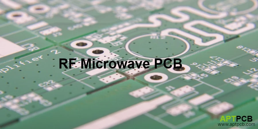
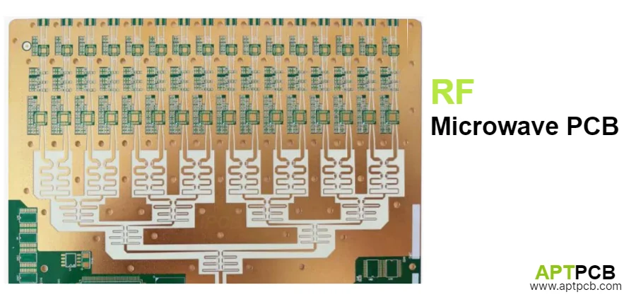
RF and microwave printed circuit boards form the backbone of modern communication systems, defense electronics, and scientific instrumentation operating at frequencies where wavelengths become comparable to circuit dimensions requiring fundamentally different design and manufacturing approaches than conventional circuits. These specialized boards demand precise control of transmission line geometries, material properties, and fabrication processes enabling reliable system performance across the frequency spectrum.
At APTPCB, we manufacture RF microwave PCBs with comprehensive expertise implementing advanced substrates, precision fabrication, and RF testing. Our capabilities support RF high frequency PCB applications from MHz-range RF through millimeter-wave frequencies with validated processes ensuring consistent performance.
Bridging RF and Microwave Frequency Domains
RF and microwave applications span overlapping frequency ranges with distinct design considerations and manufacturing requirements. Understanding the characteristics of each frequency regime guides appropriate material selection, circuit topology, and fabrication approach. Inadequate frequency-range understanding causes inappropriate material selection limiting performance, circuit topologies unsuited to operating frequency, or manufacturing tolerances insufficient for frequency requirements — directly impacting design success and system performance.
At APTPCB, our manufacturing addresses the full RF through microwave frequency spectrum.
Key Frequency Range Considerations
- RF Range (3 kHz - 3 GHz): Lumped element circuits remain practical for many applications with transmission line effects becoming important for longer interconnects and higher frequencies within this range.
- Lower Microwave (1-10 GHz): Distributed circuit techniques essential with transmission line theory governing signal propagation through controlled impedance high frequency PCB designs.
- Upper Microwave (10-40 GHz): Demanding substrate selection and precision fabrication with quarter-wave structures measured in millimeters requiring tight dimensional control.
- Millimeter-Wave (30-100 GHz): Emerging 5G, automotive radar, and imaging applications with extremely short wavelengths imposing severe material and fabrication requirements through microwave RF PCB capabilities.
- Hybrid Frequency Systems: Many applications combine RF control and digital interfaces with microwave signal paths requiring mixed-technology board designs.
- Application Matching: Frequency-appropriate material selection, design rules, and manufacturing tolerances aligned with actual operating requirements.
Frequency Expertise
Through comprehensive understanding of RF through millimeter-wave requirements, appropriate technology selection, and matched manufacturing capabilities, APTPCB enables RF microwave PCBs optimized for specific operating frequency ranges.
Implementing Comprehensive Substrate Solutions
RF microwave PCB performance depends critically on substrate material selection balancing electrical properties, thermal characteristics, mechanical stability, and manufacturing processability. Different applications prioritize different properties requiring appropriate material matching. Inadequate substrate selection causes excessive losses limiting range, impedance variations degrading return loss, or reliability issues from material incompatibility — directly impacting system performance and product reliability.
At APTPCB, our manufacturing implements broad substrate capabilities addressing diverse requirements.
Key Substrate Technologies
- Glass-Reinforced PTFE: Rogers RT/duroid, Taconic TLY, and similar materials providing low loss with mechanical stability for low-loss high frequency PCB applications through GHz frequencies.
- Ceramic-Filled Substrates: PTFE and hydrocarbon materials with ceramic fillers providing enhanced thermal conductivity and tailored CTE for power applications.
- Hydrocarbon Laminates: Rogers RO4000 series and similar materials offering improved loss characteristics over FR-4 with manufacturing processes closer to standard materials.
- Thin Film Substrates: Alumina, aluminum nitride, and fused silica supporting highest frequency applications with exceptional dimensional stability.
- Hybrid Constructions: Mixed-dielectric stackups combining high-performance RF layers with cost-effective materials elsewhere optimizing performance-to-cost ratio.
- Material Characterization: Verification of dielectric constant and loss tangent ensuring material properties meet design assumptions through testing quality protocols.
Substrate Excellence
By implementing comprehensive substrate expertise, validated processing for each material type, and application-appropriate material selection guidance, APTPCB delivers RF microwave PCBs achieving target performance across diverse substrate technologies.
Mastering Electromagnetic Design Implementation
RF microwave PCB fabrication must accurately implement electromagnetic designs including transmission lines, matching networks, filters, and couplers with dimensional precision determining electrical performance. Discontinuities, transitions, and coupling structures require careful attention. Inadequate electromagnetic implementation causes impedance errors degrading matching, filter response shifts affecting selectivity, or coupling variations impacting isolation — significantly impacting circuit function and system performance.
At APTPCB, our fabrication implements precision electromagnetic structures.
Key Electromagnetic Implementation Capabilities
- Transmission Line Fabrication: Microstrip, stripline, and coplanar waveguide structures with precision trace width and spacing control achieving target impedances.
- Matching Network Elements: Quarter-wave transformers, stub matching, and distributed L-C structures with dimensional accuracy for designed impedance transformation.
- Filter Structures: Edge-coupled, hairpin, and interdigital filter geometries with coupling gaps and resonator dimensions meeting design specifications.
- Coupler Implementation: Directional couplers and power dividers with controlled coupling achieving specified power split and isolation.
- Via Transitions: Optimized transitions between transmission line types with proper ground via placement minimizing discontinuity effects through high frequency multilayer PCB fabrication.
- Waveguide Transitions: Microstrip-to-waveguide transitions with precision mechanical features enabling interface with waveguide components.
Electromagnetic Excellence
Through precision fabrication, dimensional control, and electromagnetic verification coordinated with design requirements, APTPCB enables RF microwave PCB circuits achieving designed electrical performance.
Supporting Diverse Application Requirements
RF microwave PCBs serve diverse applications from wireless communications through defense radar and scientific instrumentation with varying requirements for performance, reliability, and environmental protection. Application-specific optimization addresses unique challenges while leveraging common manufacturing capabilities. Inadequate application understanding causes designs not meeting operational requirements, insufficient environmental protection, or non-compliance with industry standards — significantly impacting product suitability and field reliability.
At APTPCB, our manufacturing supports diverse RF microwave applications.
Key Application Areas
Wireless Communications
- 5G infrastructure including massive MIMO antenna arrays requiring consistent performance across numerous identical RF paths through RF circuit board manufacturing precision.
- Satellite communications operating from C-band through Ka-band with stringent phase and amplitude requirements.
- Point-to-point backhaul links requiring low-loss transmission across extended trace lengths.
- Small cell and distributed antenna systems demanding compact multilayer constructions.
Radar Systems
- Phased array modules requiring amplitude and phase matching across production volumes for aerospace defense applications.
- Automotive radar operating 77 GHz with high-volume manufacturing and automotive quality standards.
- Weather and surveillance radar with high-power transmit chains requiring thermal management.
- Aviation systems meeting DO-254 and AS9100 requirements.
Test and Measurement
- Network analyzer standards requiring exceptional impedance accuracy and repeatability.
- Signal source output networks with minimal loss and precise matching.
- Probe systems enabling wafer and module-level RF characterization.
Application Excellence
Through application understanding, appropriate manufacturing approaches, and quality systems meeting industry requirements, APTPCB delivers RF microwave PCBs suited to specific application needs.
Implementing Precision Fabrication Processes
RF microwave PCB fabrication demands exceptional process control achieving tight tolerances on trace dimensions, plating thickness, and dielectric properties. Statistical process control monitors critical parameters ensuring consistent results. Inadequate process control causes impedance variations between boards, insertion loss inconsistencies affecting system performance, or yield issues increasing costs — directly impacting product quality and manufacturing efficiency.
At APTPCB, our fabrication implements precision process control throughout manufacturing.
Key Fabrication Process Controls
- Precision Etching: Controlled etch factor and line width achieving trace width tolerances to ±0.5 mil with statistical monitoring through high frequency PCB fabrication processes.
- Plating Uniformity: Copper thickness control within ±10% across panel surfaces maintaining impedance accuracy and via reliability.
- Dielectric Control: Lamination processes achieving specified dielectric thickness with uniformity supporting impedance control.
- Surface Finish Selection: RF-appropriate finishes avoiding magnetic losses while providing solderability for high frequency PCB assembly requirements.
- Via Processing: Precision drilling and plating with backdrilling removing stubs preventing high-frequency resonances.
- Statistical Monitoring: Control charts tracking critical parameters with capability studies verifying process performance.
Fabrication Excellence
Through precision process control, statistical monitoring, and continuous improvement supported by advanced equipment, APTPCB achieves fabrication quality meeting demanding RF microwave PCB specifications.
Ensuring Comprehensive Testing and Verification
RF microwave PCB quality verification requires thorough testing beyond standard PCB inspection including impedance verification, material characterization, and environmental testing where specified. Complete documentation supports quality assurance and customer requirements. Inadequate testing misses electrical performance issues affecting systems, while incomplete documentation complicates quality investigations — impacting product reliability and customer confidence.
At APTPCB, our testing provides comprehensive verification ensuring RF microwave PCB quality.
Key Testing Capabilities
- Time Domain Reflectometry: Impedance measurement along transmission line coupons with statistical analysis across panel positions through high frequency PCB manufacturer quality practices.
- Network Analyzer Testing: S-parameter characterization including insertion loss, return loss, and isolation when specified for critical applications.
- Material Verification: Dielectric constant and loss tangent confirmation ensuring substrate properties meet specifications.
- Dimensional Inspection: CMM verification of critical features meeting design tolerances.
- Cross-Section Analysis: Microsection examination verifying layer registration, plating quality, and via structures.
- Environmental Testing: Temperature cycling, humidity exposure, and mechanical testing validating reliability when specified.
Testing Excellence
By implementing comprehensive testing, thorough documentation, and systematic data management coordinated with quality requirements, APTPCB delivers RF microwave PCBs with verification records meeting customer and industry expectations.
Advancing Future Technology Capabilities
RF microwave PCB technology continues advancing toward higher frequencies, improved integration, and new manufacturing approaches expanding design possibilities. Material innovations, additive techniques, and heterogeneous integration push performance boundaries. Inadequate technology advancement limits addressable applications, reduces competitive capability, or constrains design options — impacting future business opportunities and customer service.
At APTPCB, our development invests in advancing capabilities.
Key Technology Directions
- Millimeter-Wave Extensions: Material and process development supporting 60 GHz, 77 GHz, and higher frequency applications.
- Advanced Integration: Techniques combining PCB, semiconductor, and packaging technologies for compact microwave modules.
- Additive Manufacturing: Exploration of additive techniques enabling new three-dimensional structures and design freedoms.
- Low-Loss Material Development: Qualification of emerging ultra-low-loss substrates extending performance boundaries.
- Fine-Line Capabilities: Advanced patterning techniques achieving finer geometries for higher frequency transmission lines.
- Process Innovation: Continuous improvement in fabrication precision, consistency, and efficiency.
Technology Leadership
Through investment in technology advancement, material qualification, and process development coordinated with customer requirements, APTPCB positions to serve emerging RF microwave PCB applications and evolving industry needs.