Telecom & 5G / Radio, transport, access

Telecom boards.Follow the signal.

RF front-ends, baseband, optical transport and access hardware require different controls. Start with the signal path and define the construction around it.
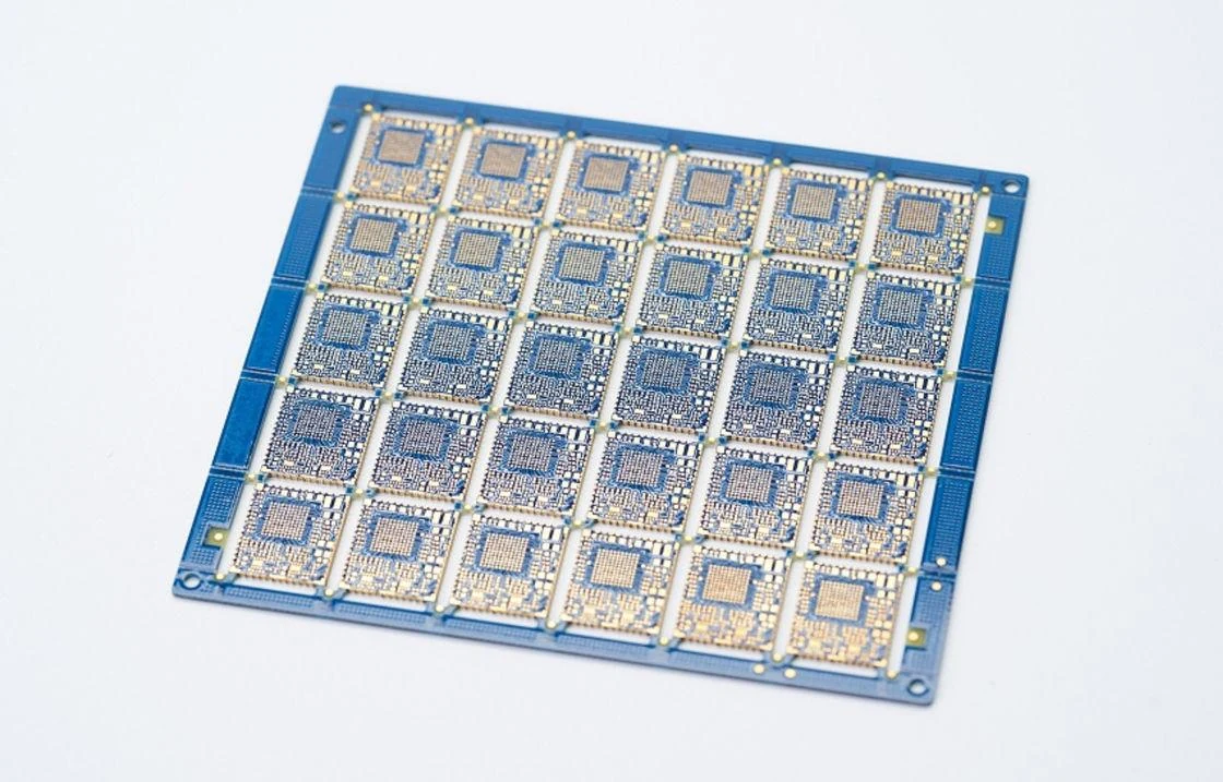
RF vs digital
Panel of blue RF module circuit boards with gold pads and plated castellated edges.

01 / Two signal domains

RF geometry and digital routing ask different questions.

01

At the radio front-end

Release material construction, RF line geometry, transitions, ground stitching and shielding interfaces.

02

At the baseband processor

Release the multilayer stackup, differential-pair requirements, dense packages and fronthaul interfaces.

As a dedicated PCB manufacturing and PCB assembly factory, APTPCB supports equipment vendors, network solution providers and ODM/OEM partners with production-ready telecom PCBs and fully assembled 5G PCBAs. We cover everything from base station PCBs, RF PCBs, antenna PCBs and small cell PCBs to core router PCBs, optical line interface boards, CPE/router PCBs, power supply PCBs, and telecom control boards used in mobile, fixed-line and converged networks.
By combining RF-capable PCB manufacturing, high-speed digital PCB processes, precise SMT assembly, and layered inspection and testing, APTPCB helps ensure your telecom and 5G PCBAs perform reliably in real networks—not just in test labs. We focus on stackup consistency, impedance control, RF behavior, solder quality and final inspection so your hardware can handle outdoor exposure, temperature swings, lightning protection schemes, long uptimes and demanding throughput with confidence.

RF Front-End, Filter & Antenna PCBs

RF front-end and antenna subsystems are critical to telecom and 5G performance. RF PCBs, filter PCBs and antenna PCBs must be manufactured with tight geometrical tolerances and appropriate materials. APTPCB manufactures RF front-end PCBs, filter and duplexer PCBs, low-noise amplifier (LNA) boards, power amplifier (PA) boards and antenna PCBs for telecom and 5G systems. With consistent RF and antenna PCB fabrication and assembly, APTPCB helps maintain predictable RF characteristics across production batches, supporting stable coverage, throughput and link budgets in telecom and 5G deployments.

Manufacturing considerations
Key RF & Antenna PCB Capabilities:
  • Controlled RF Geometry: PCB manufacturing that supports controlled-width microstrip/stripline structures, RF transitions and impedance-matched networks for RF sections
  • Material Options (as Specified): Ability to work with RF-oriented materials (where available via customer specification), or hybrid stackups combining standard and RF layers when required and feasible
  • Grounding & Shielding Practices: PCB layouts that facilitate soldered shields, ground stitching and via fences for RF isolation
  • Antenna Integration: PCBs that integrate antenna patterns or feed networks for panel antennas, small cells, CPEs and IoT devices

Scroll the table to review all columns.

5G Base Station, RRU & AAU PCB & PCBA Solutions

5G base stations, RRUs (Remote Radio Units) and AAUs (Active Antenna Units) combine RF, high-speed digital and power on tightly integrated hardware. Base station PCBs and 5G RF PCBs must meet strict RF performance, thermal and reliability requirements. APTPCB manufactures and assembles PCBs and PCBAs for 5G macro base stations, RRUs/AAUs, small cells and distributed radio units, including baseband processing boards, RF transceiver PCBs, control boards and power boards. With consistent manufacturing for 5G base station PCBs, RRU PCBs and AAU PCBAs, APTPCB helps your radio equipment deliver stable RF performance, throughput and coverage in the field, supporting operators' rollout and long-term operation of 5G networks.
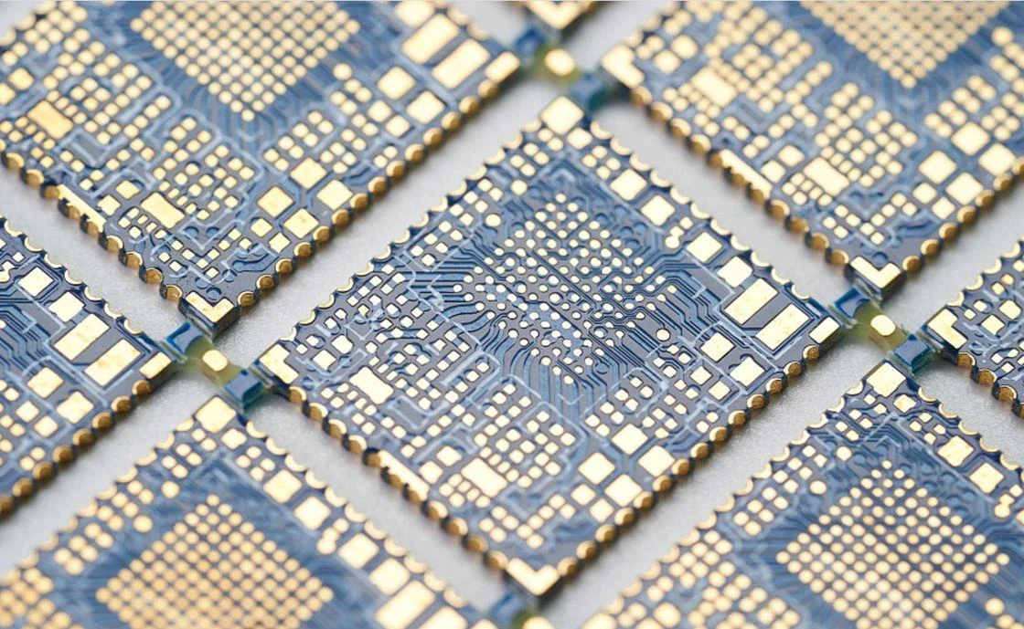
Close-up of blue RF module boards with fine traces and gold contact pads.
Manufacturing considerations
Key Base Station & RRU/AAU PCB Capabilities:
  • RF & Mixed-Signal PCB Design Support: Manufacturing support for RF layers, matching networks and filters on 5G RF PCBs and transceiver PCBs, with controlled geometries and well-defined ground reference for RF sections
  • High-Speed Baseband & Fronthaul: Multilayer base station PCBs hosting SoCs, FPGAs, ASICs and memory, with carefully controlled differential pairs for CPRI/eCPRI, Ethernet and high-speed baseband interfaces
  • Antenna Integration & Beamforming: PCBs that integrate RF front-ends with phased-array antenna elements, combining RF routing, phase-shifting networks and control circuits in AAU boards
  • Outdoor & Ruggedized Considerations: Layout and materials chosen with enclosure, sealing, coating and thermal constraints of outdoor base stations and RRUs in mind

Scroll the table to review all columns.

02 / Across the network

From antenna feed to optical transport.

Core Network, Router & Optical Transport PCBs

Core network routers, aggregation switches and packet/optical transport systems require high-speed telecom PCBs that handle many high-bandwidth ports and complex switching fabrics. APTPCB manufactures core router PCBs, aggregation switch PCBs, line card PCBs, control plane boards and optical transport line interface PCBs for telecom and data network equipment. By delivering consistent telecom router PCBs and optical transport PCBAs, APTPCB supports the backbone of telecom and 5G networks, helping ensure long uptimes, predictable throughput and easier maintenance in the field.
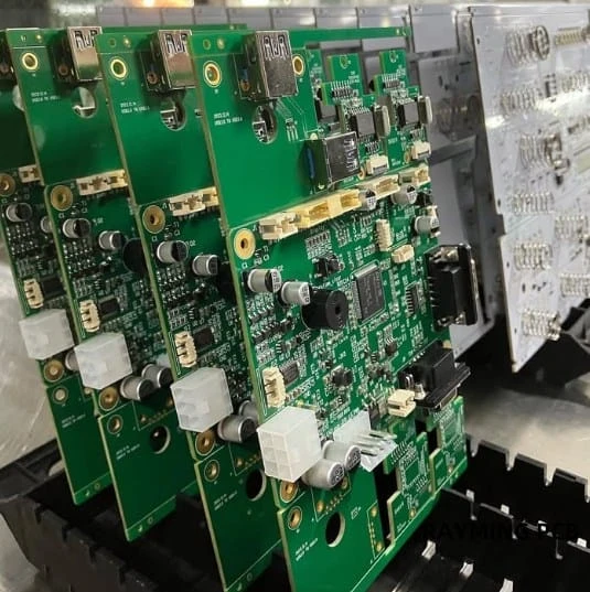
Populated networking circuit boards with integrated circuits, passive components and edge connectors
Network hardware / populated circuit boards and edge interfaces
Manufacturing considerations
Key Core & Transport PCB Capabilities:
  • High-Speed SerDes & Fabric Routing: PCB manufacturing tuned for multi-lane interfaces (e.g. 10G/25G/100G+ SerDes) and backplane/mesh fabrics with tight impedance and skew control
  • Optical Line Interface & Transponder Boards: PCBs for transponders, muxponders and coherent optics, combining analog front-end, DSP/ASIC, clocking and control circuits
  • Control & Management Boards: Multilayer PCBs for control plane CPUs, management modules, timing and synchronization boards (e.g. SyncE, IEEE 1588 PTP)
  • Backplane & Midplane PCBs: For chassis-based systems, large-format PCBs connecting multiple line cards and fabric modules with precise connector alignment and signal integrity

Scroll the table to review all columns.

03 / Access & coverage

Separate the coverage node from the customer gateway.

From indoor coverage to the customer edge

Small Cell, DAS & Indoor Coverage PCB Manufacturing

To improve indoor coverage and capacity, operators rely on small cells, distributed antenna systems (DAS), repeaters and indoor radio units. These devices require compact, efficient small cell PCBs and DAS PCB assemblies combining RF and digital functions.
APTPCB manufactures small cell PCBs, indoor 5G radio PCBs, DAS node boards and repeater PCBAs for enterprise, venue and residential coverage solutions.
Key Small Cell & DAS PCB Features:
  • Compact RF & Digital Integration: Small form-factor 5G PCBs combining transceiver chains, local processing, power control and interfaces in space-constrained designs
  • PoE & Local Power Handling: PCBs that support PoE/PoE+ power input or local DC power, including DC/DC conversion and protection circuits
  • Mounting & Thermal Considerations: Layouts compatible with ceiling, wall or furniture mounting, with appropriate heat spreading and mechanical constraints for discrete indoor units
  • Backhaul & Management Interfaces: Integration of Ethernet, fiber, or wireless backhaul along with remote management and monitoring interfaces
Through robust small cell and DAS PCBA manufacturing, APTPCB helps vendors deliver reliable indoor coverage hardware that can be deployed at scale, providing consistent performance in offices, malls, campuses and homes.

CPE, Routers, Gateways & IoT Access PCBs

Customer-premises equipment (CPE) and gateways connect end users and devices to telecom and 5G networks. CPE PCBs, router PCBs and IoT gateway PCBs must balance cost, performance and reliability.
APTPCB manufactures home and enterprise router PCBs, 5G CPE PCBs, FTTx CPE PCBs, VoIP gateway boards and industrial IoT gateway PCBAs.
Key CPE & Gateway PCB Features:
  • Integrated Wireless & Wired Connectivity: PCBs combining Wi-Fi, cellular (4G/5G), Ethernet and voice interfaces on compact boards for CPE and gateway applications
  • Low-Cost, High-Volume Manufacturing: Efficient PCB stackups and DFM-focused layouts to support cost-sensitive, high-volume CPE shipments with stable quality
  • Power & Thermal Management: Proper power distribution and thermal design for devices that may run constantly in consumer and enterprise environments
  • User Interface & Mechanical Integration: PCBs that support LEDs, buttons, displays and connectors in enclosures designed for home or office aesthetics and usability
Stable router and CPE PCBAs from APTPCB help telecom providers deliver reliable connectivity, fewer customer complaints and lower replacement rates, enhancing user satisfaction and reducing support costs.

04 / Site power & deployment

Power and mounting requirements follow the installation.

Power Supply & Site Power PCBs for Telecom & 5G

Telecom and 5G equipment depends on reliable power—both at the site (rectifiers, battery backup) and at the equipment level (DC/DC modules, PoE, local regulators). Telecom power PCBs must withstand surges, transients and continuous operation. APTPCB manufactures rectifier PCBs, DC/DC converter PCBs, power distribution PCBs, PoE injector/switch power boards and fan controller PCBs for telecom sites and network equipment. By providing consistent telecom power PCBs, APTPCB helps operators and equipment vendors maintain network uptime, protect sensitive electronics and reduce field maintenance caused by power-related failures.
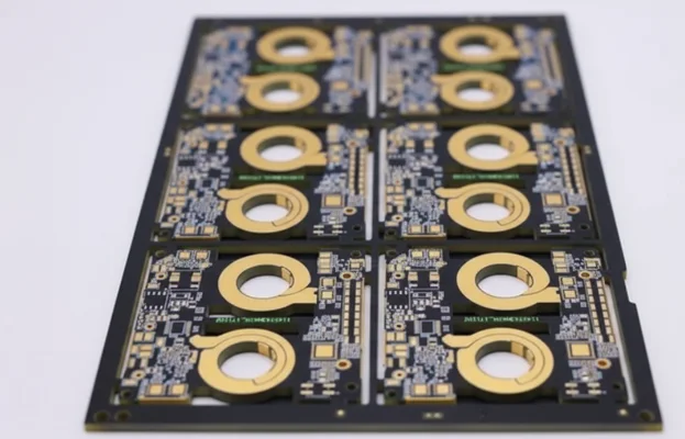
Panel of bare dark circuit boards with large plated circular features
Power-board example: assess copper features and mounting geometry.
Manufacturing considerations
Key Telecom Power PCB Features:
  • High-Current & High-Voltage Handling: Copper weights, clearances and creepage distances suitable for DC power systems commonly used in telecom sites (e.g. -48 V systems) and equipment
  • Surge & Lightning Protection Support: PCB layouts that accommodate protection components for surge, lightning and over-voltage events, especially in outdoor or tower-mounted equipment
  • Thermal Management & Reliability: Heat-spreading copper, thermal vias and mounting provisions for heatsinks to ensure long-term power stage reliability
  • Monitoring & Control Integration: Power PCBs that integrate measurement, alarms, remote monitoring and control interfaces for site power systems

Scroll the table to review all columns.

Telecom & 5G Application Categories

5G Base Stations

Baseband, RF transceiver and power boards for macro, micro and small cell base stations.

RRU & AAU Units

Remote radio units and active antenna units with integrated RF and digital functions.

Core Routers

High-speed router and switch PCBs for core network and aggregation layers.

Optical Transport

Transponder and optical line interface PCBs for packet and optical transport systems.

CPE & Gateways

5G CPE, home routers and IoT gateway PCBs for customer access and connectivity.

RF & Antennas

RF front-end, filter and antenna PCBs for wireless subsystems.

05 / Lab to deployment

Freeze the test scope before rollout.

  1. 01
    Lab samples

    Define the build

    Align RF, digital, mechanical and assembly files under the current revision.

  2. 02
    Trial hardware

    Agree the checks

    Specify hidden-joint inspection, electrical access, port bring-up and RF-chain routines as required.

  3. 03
    Production

    Control repeat builds

    Retain the accepted configuration, functional limits, labels and required lot or board records.

Testing & Quality Control for Telecom / 5G PCBAs

Telecom and 5G networks require hardware that works continuously in diverse environments. For telecom PCB assembly and 5G PCB assembly, quality control is essential. APTPCB integrates multiple inspection and test stages into the PCBA process for telecom and 5G hardware. This layered PCBA quality & testing approach supports consistent performance across prototypes, trial networks and mass deployments. For telecom and 5G customers, it means more predictable field behavior, faster rollout and reduced risk of in-service failures.
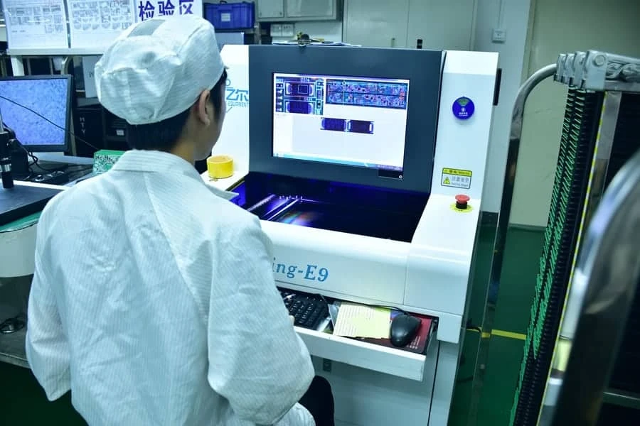
Operator reviewing a populated circuit board at an optical inspection station
Inspection coverage should follow the released package and test requirements
Manufacturing considerations
Key PCBA Quality Steps:
  • SPI (Solder Paste Inspection): Verifies solder paste volume and alignment before placement, improving solder joint quality on dense BGA and fine-pitch components
  • AOI (Automated Optical Inspection): Checks component presence, type, polarity, placement and visible solder joints after reflow
  • X-Ray Inspection (As Needed): Inspects hidden joints under BGA, LGA, QFN and power packages commonly found in baseband, switching and RF front-end boards
  • In-Circuit Test (ICT) / Flying Probe (When Designed In): Verifies electrical connectivity and component values where test access and test fixtures are available
  • Functional Test (FCT): Executes power-up, interface checks and telecom-specific test routines (e.g. link negotiation, port bring-up, RF chain checks) according to your test specification
  • Final Quality Inspection & Traceability: Confirms labeling, revision, cosmetic quality and packing, with lot-level or board-level traceability to support field quality and network maintenance requirements

Scroll the table to review all columns.

ENGINEERING REFERENCE

Additional network overview and rollout context

Key Telecom / 5G PCB Application Areas
  • 5G Base Stations & RRUs/AAUs: Baseband PCBs, RF transceiver boards, power and control modules for macro/micro base stations and active antenna units
  • Microwave & Millimeter-Wave Links: RF front-end PCBs, IF/baseband boards and control boards for point-to-point and point-to-multipoint microwave and mmWave radios
  • Core Network & Transport: High-speed router/switch PCBs, packet/optical transport boards, control and management boards for core and aggregation layers
  • Access, CPE & Gateways: GPON/EPON/FTTx PCBs, 5G CPE PCBs, home/enterprise router PCBs, industrial and IoT gateway boards
  • Power & Auxiliary Systems: Rectifier PCBs, DC/DC converter boards, power distribution PCBs, fan controller boards and site controller PCBs
From Prototype to Rollout: Partnering with APTPCB for Telecom & 5G Projects
Telecom and 5G projects typically move from lab trials to field trials, pilot deployments and finally large-scale rollouts. You need a PCB and PCBA partner who can support this entire journey for your telecom PCBs and 5G PCBAs.
APTPCB offers a complete pathway for base station PCBs, 5G RF PCBs, small cell PCBs, router/switch PCBs, CPE PCBs, RF/antenna PCBs and telecom power PCBs, from early prototype runs to stable, repeatable production.
Key Collaboration Advantages:
  • One-Stop PCB + PCBA: Fabrication and assembly under one roof simplify logistics, shorten feedback loops and accelerate design changes
  • Flexible Volumes: Support for lab samples, field-trial runs and high-volume mass production as your solution scales across regions and operators
  • Engineering Collaboration: Direct technical communication on stackup, materials, SI/RF considerations, DFM, DFT and testing, aligned with telecom and 5G requirements
  • Stable, Repeatable Quality: Process control, testing and documentation oriented toward long-term, repeatable builds—crucial for telecom networks and 5G infrastructure

ENGINEERING & PRODUCTION REVIEW

Review the next network hardware build

Share the current revision and application requirements so the manufacturing and test scope can be reviewed.

  • Board family and deployment location
  • RF material and stackup requirements
  • High-speed interfaces and mechanical drawings
  • Assembly files and functional test procedure