Factory-integrated PCB design and layout services

SCHEMATIC CAPTURE • HIGH-SPEED LAYOUT • DFM TO TURNKEY PCBA

PCB Design & Layout Services Integrated with Manufacturing

Bridge the gap between ECAD simulation and the production floor. Our custom PCB design and fabrication services pair experienced PCB designers directly with our bare-board CAM, laminate stackup, and SMT assembly engineers, delivering 100% unlocked native CAD databases and production-verified Gerber/ODB++ packages. As a factory-backed custom PCB design company, we provide full-scope PCB layout service and circuit design services under one roof.

Get an Instant Quote

Altium • Allegro/OrCAD • KiCadECAD Platforms
1–32+ Layers • HDI • Rigid-FlexLayer Capability
DDR4/5 • PCIe 4/5 • 28G SerDesHigh-Speed & RF
IPC-7351B & Stencil DFA VerifiedFootprint Standard
Live AVL & Lifecycle ScrubBOM Governance
100% Unlocked Native CAD FilesIP Ownership
Altium • Allegro/OrCAD • KiCadECAD Platforms
1–32+ Layers • HDI • Rigid-FlexLayer Capability
DDR4/5 • PCIe 4/5 • 28G SerDesHigh-Speed & RF
IPC-7351B & Stencil DFA VerifiedFootprint Standard
Live AVL & Lifecycle ScrubBOM Governance
100% Unlocked Native CAD FilesIP Ownership

Why Connect Custom PCB Design Directly to the Manufacturing Floor?

Outsourcing board layout to an independent PCB design company, standalone PCB design house, or external PCB layout company that operates separately from fabrication often shifts schedule risk from the CAD workstation to the factory pre-production gate. A layout that passes desktop DRC rules can still stall in CAM review over unavailable prepreg glass styles, unroutable 0.4 mm BGA microvia aspect ratios, or footprints whose Manufacturer Part Numbers (MPNs) are on 26-week allocation.

At APTPCB, our PCB design services embed actual factory process capabilities into the ECAD constraint manager before the first trace is routed. Every PCB designer and PCB layout engineer on our team works alongside the CAM engineers who plan multilayer PCB stackups, the procurement specialists who manage PCBA component sourcing, and the process engineers who run turnkey PCB assembly.

Which Level of Printed Circuit Board Design Services Fits Your Project?

Select the engagement tier that matches your current documentation readiness and internal engineering bandwidth.

Engagement TierBest Fit ScenarioCustomer Inputs RequiredWhat Our PCB Designers DeliverPrimary Schedule Driver
1. Concept-to-Layout (Full Custom Circuit Design + Layout)New hardware NPI or teams without an in-house circuit board designer or circuit design company partner.System block diagram, power rail budget, interface list, and target enclosure dimensions.Architecture review, schematic capture, ERC check, AVL-scrubbed BOM, 2D/3D layout, and full manufacturing release package.Key IC selection approval and mechanical outline freeze.
2. Netlist-to-Gerber (PCB Design and Layout Services)Engineering teams with a completed schematic needing a dedicated PCB layout designer or PCB board designer for complex routing.Verified native schematic (Altium, OrCAD, KiCad), preliminary BOM, and 2D/3D mechanical DXF/STEP.Stocked laminate stackup & impedance modeling, 3D placement check plot, constraint routing, SI/PI verification, and ODB++/Gerber X2 outputs.Total pin count, layer count, and high-speed bus constraint density.
3. Legacy Respin & EOL Redesign (PCB Designing Services)Existing product blocked by obsolete/NRND silicon, EMC test failures, or cost-reduction goals.Legacy schematic, Gerbers, BOM with EOL line items, or compliance failure report.Drop-in or functional circuit updates, footprint migration, layout updates, and regression DFM/DFA verification.Scope of schematic changes and fixed mechanical keep-outs.
4. Pre-Fab DFM, Stackup & Library Audit (Reliable PCB Design Service Gate)In-house designer PCB database complete; team wants factory sign-off before releasing tooling.Native CAD or ODB++/IPC-2581 + BOM + Pick-and-Place centroid (XYR).Live core/prepreg stackup alignment, impedance trace width tuning, IPC-7351 pad check, and BOM lifecycle scrub.Returned alongside fabrication and turnkey quotation review.

How Factory-Integrated PCB Design Engineering Prevents EQs and Respins

When evaluating PCB design companies or circuit board design companies, the decisive question is when physical manufacturing rules enter the layout. When a standalone PCB design firm uses generic laminate tables, the fabricator often has to modify trace widths or dielectric thicknesses during CAM review, invalidating your high-speed signal integrity simulations.

Our printed circuit board designers lock four manufacturing baselines up front: (1) real-stock laminate and prepreg selection for standard FR-4, High-Tg, Rogers RF laminates, and Panasonic Megtron; (2) laser microvia and VIPPO aspect-ratio alignment with our HDI PCB manufacturing lines; (3) IPC-7351B land pattern and stencil aperture area-ratio checks (≥ 0.66) for fine-pitch BGA and QFN assembly; and (4) live component stock and packaging suffix (-TR) verification before footprint assignment.

Technical Capability Envelope Across High-Speed, RF, HDI, Power, and Rigid-Flex

Our PCB layout design services cover simple two-layer industrial controllers through 32-layer high-speed backplanes. Specific process windows and material grades are confirmed at quotation.

Design DisciplineSupported Interfaces & Board StructuresKey Layout, SI/PI & DFM Controls Applied
High-Speed Digital & SerDes LayoutDDR4/DDR5 fly-by & clamshell, PCIe Gen 4/5, USB4, 10G/25G/100G Ethernet, MIPI CSI/DSI.Matched electrical length and intra-pair skew tuning, solid reference planes, anti-pad optimization, backdrill stub removal, and spread-glass weave mitigation.
HDI & Fine-Pitch Miniaturization0.35 mm to 0.50 mm pitch BGA/WLCSP, Type I/II/III HDI, 1+N+1 to 4+N+4 microvias, Via-in-Pad Plated Over (VIPPO).Laser microvia aspect ratio control (≤ 0.75:1), dog-bone vs. VIPPO escape routing, and symmetrical copper distribution to limit reflow warpage (≤ 0.75%).
RF, Microwave & Hybrid StackupsSub-6 GHz 5G, Wi-Fi 6E/7, GNSS, 24/77 GHz radar, hybrid PTFE/Rogers + FR-4 stackups.Microstrip and grounded coplanar waveguide (GCPW) impedance modeling, via-fence shielding, cavity isolation, and solder mask keep-outs on RF lines.
Power Electronics & Heavy CopperBMS, motor drives, EV chargers, solar inverters, 2 oz to 10 oz copper, metal-core (MCPCB) thermal layouts.High-current polygon sizing per IPC-2152, high-voltage creepage and clearance slots per IEC 62368-1 / UL 60950-1, and thermal via arrays under power MOSFETs.
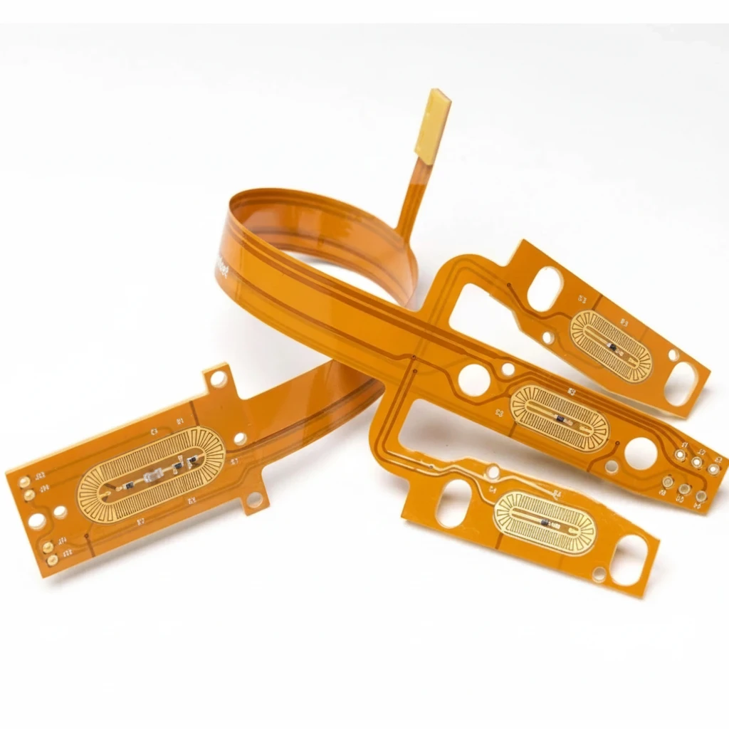
Flex & Rigid-Flex InterconnectsDynamic and static flexible circuits, multi-zone rigid-flex PCBs, ZIF tails, wearable enclosures.Neutral bend-axis routing, staggered conductors across layers, teardrop pad transitions, cross-hatched reference shields, and coverlay/stiffener overlap rules.

What Drives Custom PCB Board Design Cost and Turnaround Time?

When comparing circuit board layout services or requesting a quote for custom circuit board design, engineering hours scale primarily with pin count, constraint complexity, and mechanical density.

Cost & Schedule DriverStandard BaselineHigh-Complexity MultiplierHow to Optimize Cost & Schedule
Pin Count & Component Density< 300 pins, ≥ 0.8 mm pitch packages, single-sided or relaxed placement.> 1,500 pins, double-sided placement, 0.4 mm pitch BGAs, tight component height limits.Supply verified ECAD schematic symbols and approved IPC-7351 footprints at project kickoff.
High-Speed & Impedance BusesClock speeds < 100 MHz, standard GPIO/SPI/I2C/UART nets.Multi-channel DDR4/DDR5, high-speed SerDes lanes, strict length/phase matching (±2 to 5 mil).Provide a net-class constraint table (target Ω, max length, skew budget) before placement freeze.
Layer Count & Via Architecture2 to 6 layers, standard plated through-hole (PTH) vias only.8 to 32+ layers, sequential lamination blind/buried vias, VIPPO, or hybrid laminates.Allow our CAM and layout team to propose a stocked factory stackup before locking board thickness.
Mechanical & Enclosure ConstraintsStandard rectangular contour and edge-mounted connectors.Complex 3D enclosure profile, rigid-flex folding zones, multi-board mating headers.Provide a clean 3D STEP enclosure model and fixed connector coordinate DXF on Day 1.
Schematic & BOM ReadinessERC-clean native schematic + active MPNs with second-source alternates.Block diagram or legacy PDF schematic requiring full capture and component selection.Split schematic capture sign-off (Milestone 1) from PCB layout routing (Milestone 2).

5-Gate Workflow for PCB Layout and Design Services

Gate 1: Architecture, ERC & BOM Scrub

Our PCB design engineer reviews your schematic (or captures it from your block diagram), verifies Electrical Rules Checks (ERC), and scrubs every MPN against authorized distributor stock.

  • •Flag NRND/EOL parts before footprint assignment
  • •Confirm power tree and level-shifting logic

Gate 2: Real-Stock Stackup & Impedance Lock

Together with fabrication CAM, we build a balanced layer stackup using stocked cores and prepregs, calculating exact trace widths for 50 Ω, 85 Ω, 90 Ω, and 100 Ω controlled-impedance lines.

  • •2D field-solver impedance modeling
  • •Symmetrical press structure to prevent bow and twist

Gate 3: 3D Placement & Thermal Floorplan

We import your enclosure STEP model, lock fixed connectors and mounting holes, and partition analog, RF, high-speed digital, and switching power zones for your review before routing.

  • •3D ECAD-MCAD collision verification
  • •Customer placement sign-off prior to trace routing

Gate 4: Constraint Routing, SI/PI & DFM Audit

Our circuit board designers route high-speed trunks, match differential pair lengths, optimize return-path stitching vias, and run full CAM DFM and SMT DFA verification.

  • •Zero unrouted nets and clean DRC verification
  • •Solder mask dam, thermal relief, and stencil ratio audit

Gate 5: Unlocked CAD Handoff & Turnkey Launch

You receive 100% unlocked native ECAD files plus complete manufacturing outputs, ready for immediate bare-board fabrication and turnkey SMT assembly under one roof.

  • •Native Altium / Allegro / KiCad + ODB++ / Gerber X2
  • •Direct transition to NPI prototype build

Complete Engineering Deliverables & RFQ Input Checklist

Every custom PCB design service project concludes with full IP transfer. Use the table below to see what to submit for quoting and what you receive at sign-off.

StageDocument / File PackageAccepted / Delivered FormatsEngineering Purpose
Send with RFQSchematic or System Block DiagramAltium, OrCAD/Allegro, KiCad, or searchable PDF + netlistDetermines pin count, net count, and whether schematic capture is required.
Send with RFQPreliminary Bill of Materials (BOM).xlsx or .csv with Manufacturer & MPNAllows footprint verification, package sizing, and live component stock check.
Send with RFQMechanical Outline & Enclosure Constraints2D DXF/DWG and 3D STEP modelLocks board contour, mounting holes, fixed connector coordinates, and height keep-outs.
Send with RFQTarget Design SpecificationPDF / Markdown / Form notesDefines target layer count, impedance buses, operating temp, IPC Class 2/3, and prototype quantity.
Delivered to YouUnlocked Native ECAD Database & LibrariesNative Altium (.PcbDoc), Allegro (.brd), or KiCadGives your team 100% IP ownership for future revisions with zero vendor lock-in.
Delivered to YouIntelligent CAM & Fabrication PackageODB++, IPC-2581, Gerber X2/RS-274X, Excellon DrillPre-verified against factory etching, drilling, and solder mask registration windows (viewable in our Gerber Viewer).
Delivered to YouAssembly & Sourcing PackageScrubbed BOM (.xlsx), Centroid (XYR), Assembly PDF, 3D STEPReady for immediate feeder programming on our NPI and small-batch PCBA lines.

Clear Responsibility Boundaries from Layout to Production

Whether you engage us for standalone printed circuit board layout services, circuit board design & layout services, or a bundled turnkey PCB board design services and assembly program, responsibilities are defined before work begins. Our engineering team is responsible for executing schematic capture, library creation, stackup modeling, layout routing, and DFM/DFA verification against the agreed specification and customer sign-off gates. Final system-level functional, firmware, EMC, and regulatory qualification of the end product remains with your product team unless specific testing protocols are expressly included in your contract. Exact engineering schedules, milestone deliverables, and applicable quality certifications are confirmed at quotation based on your project scope.

Frequently Asked Questions

Which ECAD software platforms do your PCB designers support?

Our printed circuit board designers work natively in Altium Designer, Cadence Allegro / OrCAD, and KiCad. At project completion, we hand over the unlocked native schematic and layout databases alongside ODB++, IPC-2581, Gerber X2, Excellon drill, 3D STEP, and pick-and-place centroid (XYR) files.

Do I retain full ownership of the native CAD files?

Yes. You retain 100% intellectual property (IP) and file ownership of every schematic, custom library footprint, and layout database created under our custom PCB design services. All native CAD files and manufacturing packages are delivered unlocked with no vendor lock-in.

Why choose a manufacturer's PCB design service over a standalone design house?

A standalone PCB design house or third-party PCB layout company often routes boards using textbook defaults that trigger Engineering Queries (EQs) when sent to a factory, such as unstocked prepreg thicknesses, invalid microvia aspect ratios, or footprints that do not match the ordered MPN suffix. Because our PCB design engineering team works directly with our CAM and SMT engineers, your layout is verified against live laminate press stackups, stencil rules, and component stock before release.

How are PCB design cost and turnaround time calculated?

Engineering fees and turnaround time scale with total pin count, net count, layer count, high-speed length/impedance constraints, and mechanical enclosure complexity. We quote a fixed project price or milestone schedule after reviewing your schematic, BOM, and board outline.

Can you redesign an existing board to replace obsolete or EOL components?

Yes. Under our legacy redesign and respin scope, our circuit board designers identify active pin-compatible or functional replacements for NRND/EOL silicon, update the schematic and land patterns, re-verify signal and power integrity, and preserve your existing enclosure mounting coordinates.

What files should I send to request a custom PCB design quote?

Send your native schematic or PDF schematic (or system block diagram if schematic capture is needed), preliminary BOM with MPNs, 2D/3D mechanical board outline (DXF or STEP), and target specification (layer count, controlled-impedance interfaces, operating temperature, and prototype quantity).

Need custom PCB design or layout support?

Share your schematic, block diagram, preliminary BOM, and mechanical outline—our engineering team will return a scoped design proposal, stackup recommendation, and lead time within one business day.