PCB Technology Blog

Technical Insights

APT PCB Technology Blog

Expert insights on PCB manufacturing, assembly excellence, and cutting-edge electronic technologies

Get an Instant Quote

TechnologyMay 8, 2026

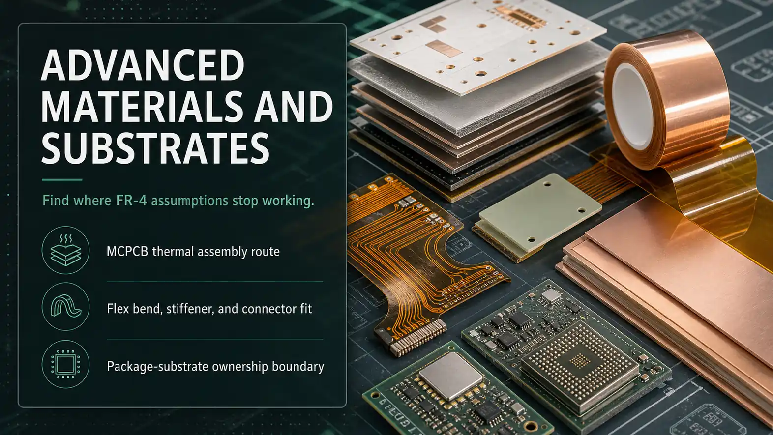
Advanced PCB Materials and Substrates Guide: MCPCB, Flex, and Package-Substrate Review

A practical engineering guide to advanced PCB materials and substrates: how metal-core boards, flex structures, and package substrates change the manufacturing route, assembly route, and release boundary before first build.

TechnologyMay 8, 2026

High-Speed and RF PCB Manufacturing Guide: Stackup, Materials, Transitions, and Validation

A practical engineering guide to high-speed and RF PCB manufacturing: how stackup direction, material scope, local transitions, shielding, and layered validation shape release readiness before pilot or mass production.

TechnologyMay 8, 2026

The Ultimate Guide to PCB Cost Reduction: Drivers, Pricing & Optimization

A practical engineering guide to PCB cost reduction: how BOM clarity, stackup choices, HDI scope, surface finish, panel strategy, and DFM review affect quote complexity before RFQ.

TechnologyMay 8, 2026

PCB Design for Manufacturing Guide: DFM Review, Test Strategy, and Release Readiness

A practical engineering guide to PCB design for manufacturing: how release clarity, fabrication route, test strategy, and reliability evidence should be reviewed together before quote, pilot build, and volume release.

TechnologyMay 8, 2026

PCB Industry Solutions: Medical, Industrial Control, Advanced Interfaces, and Power Electronics

A practical industry-solutions guide to PCB and PCBA programs: how medical, industrial control, advanced-interface, and power-electronics projects expose different board-level risks before quote and release.

TechnologyMay 8, 2026

Quick-Turn PCB Prototype Guide: Lead Time, DFM Review, and What Changes in Fab

A practical engineering guide to quick-turn PCB prototypes: how lead time, DFM intake, factory routing, prototype validation, and shipping posture change compared with the standard release path.

MaterialsMarch 20, 2026

Rogers RO3006 RF PCB: Design on a Dk 6.15 Substrate

Rogers RO3006 RF PCB design guide: 50 ohm trace geometry on Dk 6.15, insertion loss budgeting, surface finish selection, and hybrid stackup configuration.

ManufacturingMarch 19, 2026

Rogers RO3003 PCB Fabrication: Process Steps, PTFE Challenges, and Solutions

A practical engineering guide to Rogers RO3003 PCB fabrication. Covers PTFE drilling parameters, vacuum plasma desmear, hybrid lamination CTE management, and IPC Class 3 via plating for 77GHz radar boards.

MaterialsMarch 18, 2026

Rogers RO3003 High-Frequency PCB: When It's Required

When does a design actually need Rogers RO3003? A frequency-driven decision framework comparing RO3003 against FR-4 and RO4350B for high-frequency PCB selection.

ManufacturingMarch 17, 2026

Rogers RO3006 PCB Fabrication: Process Steps and Controls

Rogers RO3006 PCB fabrication: plasma desmear, modified drilling, LDI for narrow Dk 6.15 traces, hybrid lamination, and IPC Class 3 plating requirements.

ManufacturingMarch 16, 2026

RO3003 PCB Cost: Key Cost Drivers and Proven Reduction Strategies

RO3003 PCB cost breakdown: raw material pricing, hybrid stackup savings, and three strategies to reduce cost by 30–45% without compromising RF electrical performance.

MaterialsMarch 15, 2026

Rogers RO3003 PCB: Material Properties, Specs, and When to Use It

Everything engineers need to know about Rogers RO3003 PCB material: Dk 3.00 ± 0.04, Df 0.0010, TcDk -3 ppm/°C, and how these properties solve 77GHz automotive radar design problems.

...