01
Dedicated NPI Engineering Team
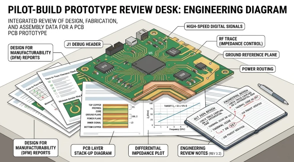
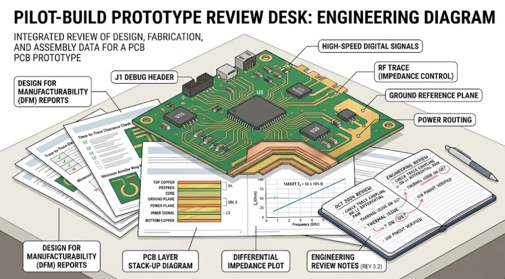
Your project isn't placed in a general queue. A dedicated CAM engineer and project manager follow your design from EVT through mass production, ensuring continuity of knowledge. You have direct communication lines to discuss stack-ups, tolerances, and design trade-offs.