Selection of ENIG, HASL, ENEPIG and OSP PCB surface finishes

Selection and specification

PCB surface finishes for soldering, contact and storage

A PCB surface finish protects exposed copper until assembly and defines the interface used for soldering, wire bonding or electrical contact. APTPCB aligns ENIG, ENEPIG, lead-free HASL, OSP, immersion silver, immersion tin or hard gold with your components, assembly flow, environment and required evidence.

7 options
Solder and contact finishes
4 inputs
Assembly, contact, storage, control
RFQ baseline
Specification before release

Get an Instant Quote

ENIGPlanar solderable surface
ENEPIGSoldering and wire bonding
LF-HASLGeneral assembly
OSP / Ag / SnNickel-free options
Hard goldWear contacts
SelectiveMultiple functions on one PCB
ENIGPlanar solderable surface
ENEPIGSoldering and wire bonding
LF-HASLGeneral assembly
OSP / Ag / SnNickel-free options
Hard goldWear contacts
SelectiveMultiple functions on one PCB

Comparison

Which PCB surface finish fits which function?

Use this table to shortlist options, not to release a design. The standard, revision, layer system, assembly process and acceptance criteria still belong in the purchase data.

FinishSystem / referencePlanarityTypical functionDefine before approvalMain limitation
Lead-free HASLLead-free solder leveled by hot airLimitedGeneral SMT/THT assembly where height variation is acceptableComponent pitch, thermal load, hole and pad geometryNot planar; very small pads require DFM review
ENIGElectroless nickel / immersion gold; IPC-4552HighFine-pitch SMT, planar pads, qualified aluminum wire bondingNi/Au layers, solder or bond process, corrosion controlThe solder joint forms on nickel, so process control matters
ENEPIGElectroless nickel / palladium / immersion gold; IPC-4556HighQualified combinations of soldering and gold or aluminum wire bondingWire, layer system, pad function and control planMore process steps and higher metallization cost
Immersion silverDisplacement silver; IPC-4553HighFine-pitch SMT and RF when a nickel-free surface is relevantSulfur exposure, packaging, handling and RF validationSensitive to tarnish and unsuitable storage environments
Immersion tinDisplacement tin; IPC-4554HighFine-pitch SMT and selected press-fit systemsFinished hole, pin, storage and thermal sequenceSurface and intermetallic layers change with time and heat
OSPOrganic protection over copperVery highCost-controlled SMT production with a short managed flowReflow cycles, floor life, test access and handlingProtection is sensitive to heat, abrasion and contamination
Electrolytic hard goldElectrolytic nickel / alloyed goldFunction-specificEdge fingers and mating, switching or sliding contactsThickness, hardness, bevel, contact load and wear testDesigned for mechanical contact, not general solderable pads

Supplier data-sheet thickness ranges are starting points. The approved drawing, agreed standard revision and documented function of each pad remain the release baseline.

Buyer decision

What APTPCB needs to select a PCB surface finish

The decision does not start with ‘ENIG or HASL?’ It starts with the function of every exposed copper area. Identify solder pads, wire-bond zones, press-fit holes, edge fingers, test points and RF-critical conductors. Add the smallest pitch, package types, reflow or selective-solder sequence, planned storage and any contact or environmental load.

APTPCB reviews those inputs with the stack-up, material and fabrication data. On an HDI board, planarity and small pads may dominate; on a high-frequency PCB, finish, copper roughness and geometry must be evaluated together; for press-fit holes, the complete hole-and-pin system matters. The output should be a measurable specification, not a generic recommendation.

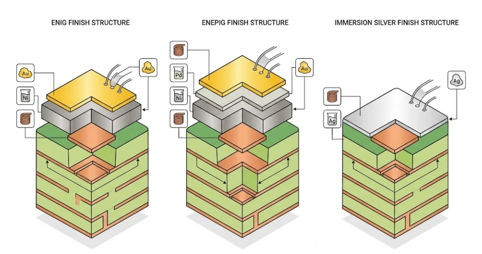
ENIG, ENEPIG and immersion silver layer systems on PCB pads

ENIG

When electroless nickel immersion gold is the right choice

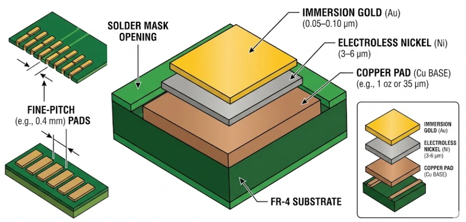
ENIG is a planar solderable finish made from electroless nickel followed by a thin immersion-gold layer. Gold protects the nickel until assembly and dissolves into the solder; the metallurgical joint then forms between solder and nickel. IPC-4552 covers this layer system.

Consider ENIG when:
small SMT pads need a planar surface, storage and assembly logistics are controlled, or a qualified aluminum-wire process is planned. ENIG does not replace bond or reliability qualification: wire, pad metallurgy, process window and required evidence must be specified.

Control black-pad risk:
this failure mode is associated with an unsuitable nickel surface or corrosive attack during gold deposition. A claim alone does not remove it. Qualified chemistry, bath control, layer requirements, process checks and product-risk testing provide the actual control strategy.

Evaluate mechanical load too:
because the solder joint forms at the nickel-tin interface, products exposed to bending, shock or vibration should not be released on planarity alone. Layout, pad definition, mechanical support and real loading belong in the reliability assessment.

Planar ENIG pads for fine-pitch BGA and QFN assembly

Lead-free HASL

When lead-free HASL remains a practical choice

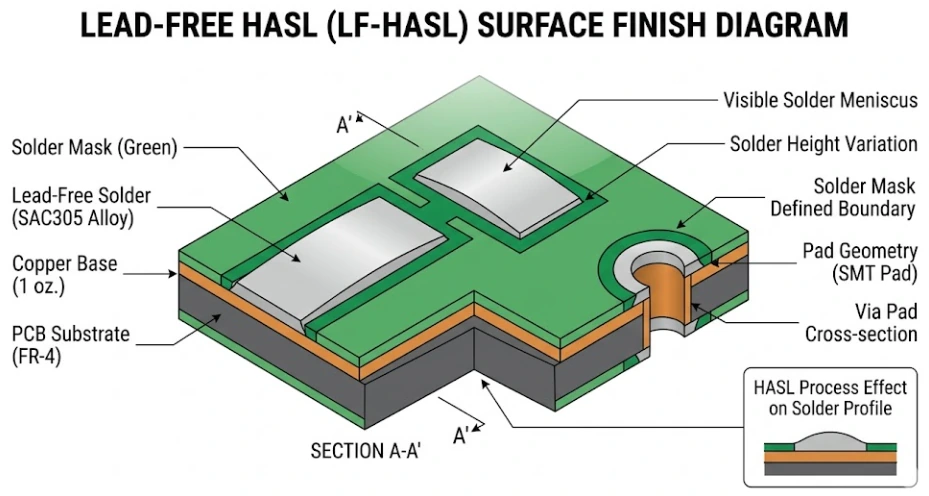
Lead-free HASL coats exposed copper with lead-free solder, then removes excess solder by hot-air leveling. It produces a well-understood solderable surface, but deposit height varies more than with a planar chemical finish.

Good candidates:
general industrial electronics, prototypes and THT or mixed-technology boards where component pitch, paste printing and coplanarity tolerate a solder meniscus. Cost comparisons must keep design, inspection and packaging scope equal.

Limits to review before quotation:
very small pads, fine-pitch BGAs, thin or thermally sensitive constructions and tightly controlled contacts may rule out lead-free HASL. The thermal load and variable solder distribution belong in DFM review.

Avoid false thickness precision:
one nominal value poorly describes a deposit driven by geometry. The drawing and acceptance plan should instead define complete wetting, acceptable planarity and critical functional areas.

Lead-free HASL pads showing geometry-dependent solder distribution

Special functions

Use ENEPIG, silver, tin, OSP and hard gold for the right job

Each finish supports a different function. Keep the decision tied to the pad and the process that follows.

01

ENEPIG: combine soldering and wire bonding

ENEPIG adds palladium between electroless nickel and immersion gold; IPC-4556 covers the system. It is often evaluated when one PCB combines soldered components with gold or aluminum wire. Wire material, layer system, bonding window and acceptance test still require project qualification.

02

Immersion silver: planar and nickel-free

Immersion silver under IPC-4553 forms a planar layer directly on copper. It can suit fine-pitch SMT and critical RF conductors. Sulfur exposure, finger contact, packaging and time to assembly belong in the specification.

03

Immersion tin: coordinate assembly and press-fit

Immersion tin under IPC-4554 provides a planar solderable surface and may suit selected press-fit systems. Suitability also depends on finished hole size, barrel copper, pin geometry, insertion force and storage history. PCB and connector must be validated together.

04

OSP: keep the production chain short and controlled

OSP protects copper with a very thin organic layer while preserving planar pads. It suits cost-sensitive SMT production when storage, handling and thermal cycles are tightly managed. Floor life, rework and electrical contact requirements should be agreed before volume release.

05

Hard gold: optimize wear, not solderability

Electrolytic hard gold is intended for edge fingers and mating, switching or sliding contacts. The drawing should define nickel and gold requirements, contact zone, hardness or alloy, bevel, allowable over-plating and expected load. A generic cycle count does not replace system qualification.

06

Selective finishes: separate pad functions

More than one finish can share a board, such as ENIG on solder pads and hard gold on edge fingers. Explicit zones, maskable transitions, a realistic sequence and separate acceptance criteria are required before quotation approval.

Selection matrix

Choose the finish from the most critical function

Start with the strictest requirement. When several rows apply, the specification must resolve the trade-off explicitly.

RequirementFirst candidatesRelease question
Fine-pitch BGA / QFNENIG, ENEPIG, immersion silver or tin, OSPWhat planarity, reflow sequence, storage and rework does the assembler require?
Standard assembly with substantial THTLead-free HASL or ENIGIs HASL height variation acceptable on every functional pad?
Gold and/or aluminum wire bondingENEPIG; ENIG for selected aluminum-wire processesWhich wire, bond process and acceptance test are qualified?
RF or microwave conductorsImmersion silver, OSP or a validated alternativeHow does the finish affect the field and measured insertion loss?
Press-fit interfaceImmersion tin or an approved alternativeAre finished hole, layer system and pin-maker requirements aligned?
Edge fingers / mating contactsElectrolytic hard goldWhich thickness, hardness, bevel geometry and load must be demonstrated?
Cost-sensitive SMT productionOSP or lead-free HASLIs the flow short enough, and are planarity and rework controlled?
Long or uncertain logisticsENIG, ENEPIG or a project-validated finishWhich packaging, storage and reinspection rules actually apply?
Multiple pad functionsSelective finish combinationAre zones, sequence and separate acceptance criteria fixed in the drawing?

This matrix does not replace component data or assembler qualification. It structures the technical review before RFQ and DFM.

What a release-ready PCB surface finish specification contains

1. Functions and zones

Identify surfaces used for soldering, bonding, press-fit insertion, mating contact or critical RF conduction. For selective finishes, transitions, masking and allowable overlap must be unambiguous in the fabrication data.

2. Layer system and standard

State finish, standard and revision, then target, minimum or range values where function requires them. Common references include IPC-4552 for ENIG, IPC-4553 for immersion silver, IPC-4554 for immersion tin and IPC-4556 for ENEPIG.

3. Downstream process and environment

Describe soldering, reflow cycles, wire type, press-fit system, storage, packaging and any critical environment. Without this context, a chemically feasible finish cannot be declared suitable for the product.

4. Acceptance and evidence

Specify visual inspection, thickness measurement, solderability under IPC J-STD-003, microsection, wire-bond, contact or RF testing only as needed. Sampling, points, limits and report format belong in the purchase order.

Writing only ‘ENIG’ or ‘hard gold’ does not make quotations comparable. A controllable specification connects pad function, layer system, limits, test methods and deliverables.

How surface finish affects RF and signal integrity

Nickel in the field region

A nickel barrier in a strongly excited conductor region can change measured RF behavior. ENIG or ENEPIG are not automatically excluded, but they should be included in the model with geometry, frequency and insertion-loss target.

Nickel-free options

Immersion silver or OSP are often evaluated when a nickel-free conductor surface is preferred. Their value disappears if tarnish, storage, handling or assembly are not controlled.

Measure instead of claiming

For a loss-critical channel, use the same stack-up, copper profile and finish in the solver and measurement chain. Coupons, resonators or other agreed structures may be required; product evidence decides, not an ‘RF optimized’ label.

Treat wear contacts separately

A wear contact may require hard gold while an RF conductor needs another surface. Selective metallization separates those functions when layout and process sequence allow it.

At high frequency, current concentrates near the conductor surface. Copper roughness, geometry and metallization can therefore affect loss and impedance together; the finish name alone does not create a universal ranking.

Applications

Choose the finish by product risk, not industry label

Industry name alone does not decide the finish. Real assembly, contact, environment and evidence requirements do.

High-density SMT

Planarity and paste printing

For small BGA, QFN and LGA pads, a planar surface and stable paste deposit come first. ENIG, ENEPIG and other planar options are then compared by storage, reflow and rework needs.

Industrial and automotive

Change control and evidence

Approved drawings, controlled revisions, lot traceability and agreed reports matter more than a sector-based recommendation. Product and system qualification remain the program owner's responsibility.

RF and microwave

Include finish in the stack-up

Finish, copper roughness and geometry are evaluated together. A nickel-free option may help, but it must still meet assembly, packaging and measured electrical targets.

Connectors

Separate mating contact from press-fit

Edge fingers need a hard-gold specification tied to wear. Press-fit needs a coherent hole, layer and pin system. Neither function should be confused with a general solderable finish.

Flex and rigid-flex

Account for bending and process heat

Finish, pad construction and transition into the flexible area must match real bending. Finish cannot compensate for poor geometry on a rigid-flex PCB.

Prototype to production

Do not change finish silently

A finish change between prototype and production can alter paste printing, solder joint, test contact and storage. Finish, standard revision and control plan belong in the approved baseline.

Process release

From RFQ to a controlled surface finish release

1. Verify the specification
APTPCB maps each pad function to the requested finish and checks alignment across drawing, fabrication data, standard, layer system and downstream process. Ambiguous mixed-finish boundaries or unmeasurable requirements are clarified before fabrication release.

2. Set the process and control plan
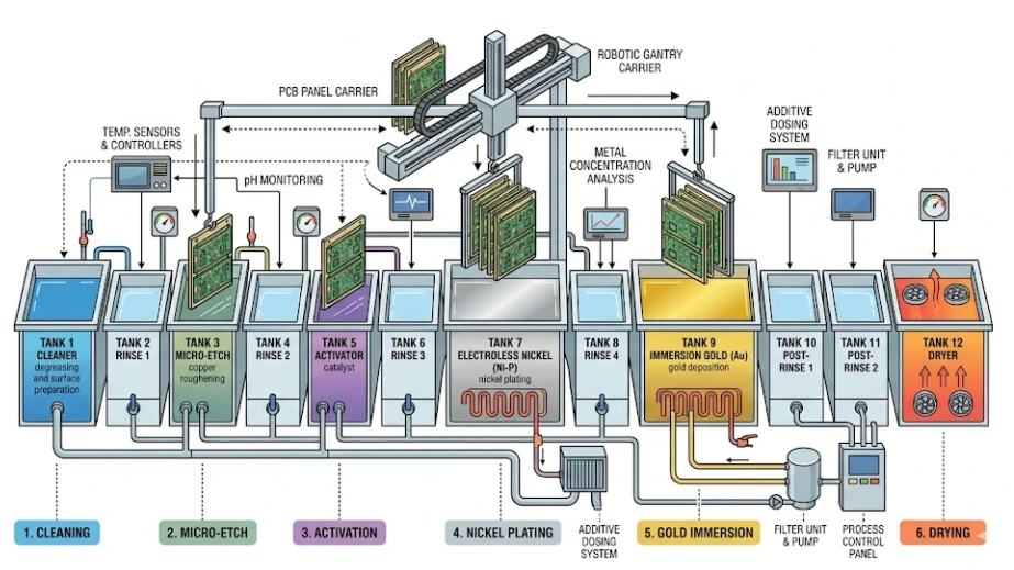
Based on finish and product risk, process parameters, measurement methods, sampling and hold points are agreed. Bath analysis, XRF, microsection or solderability are possible tools, not an automatic package for every order.

3. Define handling and packaging
Clean handling, suitable packaging and controlled conditions protect the surface until assembly. For OSP, immersion silver and immersion tin, floor life, environment and downstream process should be aligned with the assembler.

4. Reassess changes
Changing finish, chemistry source, layer system, pad function, thermal profile or bonding process can invalidate the approved basis. The program should define which changes are documentary and which require renewed qualification.

Controlled PCB surface finish process with defined release points

Cost

Compare finish costs without deleting technical requirements

Cost depends on treated area, layer system, selectivity, inspection, volume and metal pricing. A fixed multiplier is not reliable.

FinishRelative tendencyMain cost driversWhen added cost serves the design
OSPLowShort organic coating processManaged SMT production with short storage and assembly flow
Lead-free HASLLow to mediumSolder alloy, board geometry and thermal suitabilityGeneral SMT/THT assembly with acceptable planarity
Immersion tinMediumChemistry, process time, handling and packagingPlanar surface or a qualified press-fit system
Immersion silverMediumSilver chemistry, packaging and environmentPlanar nickel-free surface with controlled logistics
ENIGMedium to highMulti-step Ni/Au chemistry and layer controlFine pitch, defined storage strategy or qualified aluminum wire bonding
ENEPIGHighAdditional palladium layer and process controlQualified combination of soldering and wire bonding functions
Hard goldHigh, often selectiveGold amount, area, masking, bevel and inspectionMating, switching or sliding contacts exposed to wear

Compare quotations using the same drawing, layer system, treated areas, inspections, records and packaging. Otherwise, the lowest price is not technically comparable.

Quality assurance

Which evidence makes a surface finish release credible?

Visual inspection and coverage
Exposed copper, missing deposit, discoloration, tarnish, blistering, contamination or damaged pads are finish-related signals. Criteria and sampling should match the standard and product risk.

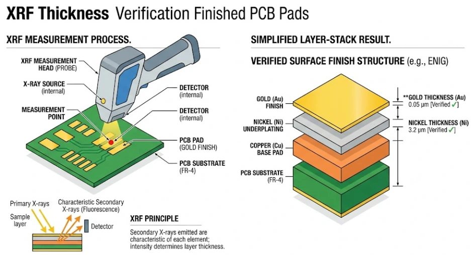
Thickness measurement
XRF can be suitable as a non-destructive method for multilayer metallic systems. Points, number of readings, analysis and limits still need definition; one reading does not prove every pad function.

Function-based testing
Depending on risk: IPC J-STD-003 solderability, microsection, bond testing, contact resistance, press-fit testing or RF measurement. The test should represent the real function and be aligned with the assembler or system owner.

Delivery records
Certificate of conformance, thickness report, test record, lot traceability or retained coupons are deliverables only when their scope and format are included in the order.

Thickness measurement used to verify a metallic PCB surface finish

FAQ

Frequently asked questions about PCB surface finishes

What is a PCB surface finish?
A PCB surface finish protects exposed copper until assembly and creates the interface used for soldering, wire bonding or electrical contact. Selection depends on pad geometry, assembly process, storage, contact function and required inspection, not price alone.
Which surface finish works for fine-pitch BGA and QFN packages?
Fine-pitch BGA and QFN packages generally need a planar surface. ENIG and ENEPIG are common candidates; immersion silver, immersion tin or OSP may also work depending on the reflow profile, thermal cycles, storage, rework and any wire-bond requirement.
What is the difference between ENIG and ENEPIG?
ENIG uses electroless nickel and immersion gold. ENEPIG adds an electroless palladium layer between nickel and gold. Palladium broadens the possible soldering and wire-bond combinations, but adds process steps and cost. Wire material, bond process and acceptance criteria still require project qualification.
Which PCB surface finish should be used for RF or microwave designs?
Immersion silver and OSP are often evaluated when a nickel-free conductor surface is preferred. No finish is best in every RF design: frequency, field distribution, trace geometry, copper roughness, storage and assembly must be included in the stack-up model and validated with agreed test structures when needed.
Can multiple surface finishes be used on one PCB?
Yes, when layout and process sequence allow it. A common example uses a solderable finish on component pads and electrolytic hard gold on edge fingers. The drawing must separate zones, layer systems, thickness requirements, masking, bevel and acceptance criteria.
How long can ENIG, OSP or immersion silver PCBs be stored?
A generic shelf-life number is not enough to release a lot. Usable storage time depends on finish, packaging, temperature, humidity, sulfur exposure, handling and prior thermal cycles. Fabricator and assembler should agree storage conditions, floor life after opening and any required solderability recheck.
Which surface finish should be specified for wire bonding?
Define wire material and bonding process first. ENIG may suit qualified aluminum-wire processes; ENEPIG is often considered for gold wire, aluminum wire or boards that combine soldering and wire bonding. Layer system, surface condition and bond parameters must be qualified with the assembler.
Which finish is suitable for press-fit connectors?
Immersion tin is often considered for press-fit systems, but finish alone does not validate the interface. Finished hole size, copper and finish in the barrel, pin geometry, insertion force, repairability and the connector manufacturer's specification determine suitability together.
What should a PCB surface finish RFQ include?
State the finish and applicable zones, standard and revision, target or minimum layer requirements, soldering, bonding, contact or press-fit function, storage and packaging needs, and expected inspection records. For RF or mixed-finish designs, include the stack-up, critical nets, masking limits and acceptance method.
Which inspection reports can be requested for a PCB surface finish?
Depending on product risk, the control plan may include visual inspection, thickness measurement, solderability testing, microsection, wire-bond or contact qualification, a certificate of conformance and lot traceability. These are not automatic deliverables: scope, sampling, measurement points, limits and report format must be agreed before fabrication release.


How to qualify a new or different PCB surface finish

Build comparable samples

Test boards should preserve pad geometry, base material, copper profile and assembly sequence. Otherwise, a difference cannot be attributed reliably to the finish.

Test the useful edge cases

Maximum planned storage, thermal cycles, smallest pads, bond areas, contact wear and RF structures are possible cases. Not every test belongs on every product, but each critical function needs named evidence.

Document the release

Standard revision, layer system, process source, test method and acceptance limit join the product baseline. A sourcing substitution must never change the approved finish silently.

An alternative finish is a process and product change, not a simple purchasing option. It must demonstrate the real soldering, bonding, contact, storage or RF function.

Global sourcing

Compare PCB surface finish quotations across sites

One technical baseline prevents regional habits or different supplier wording from producing quotations that cannot be compared.

Europe
Align the standard and drawing

Standard revision, metric thickness units, RoHS needs, packaging and fabrication notes are consolidated in one approved English-language specification.

IPCRoHSDrawing
North America
Clarify units and acceptance

Micrometers and microinches, customer standards, coupon plans, inspection reports and assembly-qualification ownership are aligned before comparison.

UnitsCouponsReports
Asia-Pacific
Control transfer to production

Prototype and production share the same finish baseline, pad functions, standard revision and inspection definition. Differences are evaluated before transfer.

TransferRevisionProduction
Global programs
One baseline, explicit changes

Multiple sites use the same drawing, limits and change process so the surface function remains controlled across repeat orders.

BaselineChangeTraceability

Request a PCB surface finish with a verifiable specification

Send Gerber or ODB++ data, stack-up, critical component list, assembly process and soldering, bonding, contact, storage and inspection needs. We review the selection and prepare a comparable quotation.

Discuss the specification