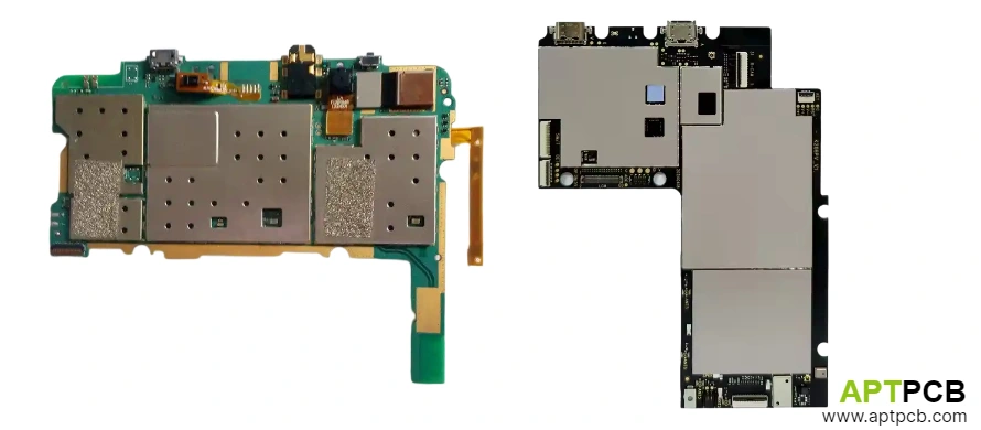
Tablet computers occupy a design space between smartphones and laptops—larger than phones but still demanding extreme thinness (typically 5-8mm total device thickness), requiring substantial battery capacity for all-day use, and integrating touch interfaces as the primary user input. The PCB design challenges reflect this middle ground: component density approaches smartphone levels for premium tablets, while display interfaces and battery management scale toward laptop complexity.
This guide examines tablet-specific PCB considerations: achieving thin stackups while maintaining signal integrity, integrating battery management for large lithium cells, implementing touch controller systems with minimal noise, routing high-bandwidth display interfaces, and manufacturing requirements that ensure quality at consumer electronics volumes.
In This Guide
- Ultra-Thin Stackup Design for Tablet Form Factors
- Battery Management System PCB Integration
- Touch Controller Routing and Noise Immunity
- Display Interface Design: MIPI and eDP Requirements
- Manufacturing Challenges for Thin Tablet PCBs
- Reliability Considerations for Consumer Tablets
Ultra-Thin Stackup Design for Tablet Form Factors
Premium tablets target total PCB thickness below 0.8mm while supporting 6-8 layers for adequate routing capacity. This thickness constraint drives selection of ultra-thin materials—50-75μm prepregs, 100-150μm cores, and careful attention to copper plating thickness that contributes to final height. Standard FR-4 constructions rarely achieve these targets; specialized thin-core materials and precise processing become necessary.
The thin stackup creates signal integrity challenges—reduced dielectric thickness narrows impedance tolerance windows, and thinner copper increases resistance and current density. Designers must balance electrical requirements against mechanical constraints, ensuring the thin assembly survives handling during manufacturing and maintains flatness under thermal stress.
Thin Stackup Design Approaches
- Material Selection: High-Tg, low-CTE thin laminates provide dimensional stability; materials like Panasonic Megtron or Isola FR408HR offer thin core options with controlled properties.
- Layer Count Optimization: Six layers typically sufficient for mainstream tablets; premium devices may require 8 layers for processor complexity—each additional layer pair adds ~0.15-0.2mm.
- Copper Weight Trade-offs: 1/3oz (12μm) or 1/2oz (18μm) copper on signal layers; inner power layers may need 1oz for current capacity despite thickness penalty—simulate power delivery to verify adequacy.
- Dielectric Thickness: Target 50-75μm prepregs between signal and reference layers; impedance calculation must account for final pressed thickness after lamination.
- Via Structure Constraints: Through-hole vias limit minimum thickness (drill aspect ratios); microvias (HDI construction) enable thinner designs by eliminating through-hole constraints.
- Stiffener Considerations: Very thin boards may require stiffeners in specific areas for component mounting or connector support—factor into overall thickness budget.
Understanding PCB stackup design principles helps optimize layer arrangement for both electrical performance and manufacturability within thickness targets.
Battery Management System PCB Integration
Tablets typically incorporate 20-40Wh lithium polymer batteries—significantly larger than smartphones, requiring robust battery management systems (BMS) for safety and longevity. The BMS circuitry may reside on the main logic board or on a dedicated battery protection board, with trade-offs between integration level, safety isolation, and serviceability.
Battery management for tablets includes cell monitoring (voltage, temperature, current), charge control (constant current/constant voltage profiles), protection circuits (overvoltage, undervoltage, overcurrent, short-circuit), and fuel gauging (state-of-charge estimation). PCB implementation must provide adequate current-carrying capacity for charge and discharge paths while maintaining isolation between high-current battery circuits and sensitive electronics.
Battery Management PCB Requirements
- Current Path Design: Charge and discharge paths carry 2-4A continuous (fast charging may exceed 10A); trace width calculation based on acceptable temperature rise—typically target <10°C rise at maximum current.
- Sense Resistor Implementation: Current sensing via low-value shunt resistors (5-20mΩ); Kelvin connection routing to sense amplifier eliminates trace resistance error.
- Protection MOSFET Placement: Battery disconnect MOSFETs positioned close to battery connection; thermal considerations for power dissipation during short-circuit protection events.
- Isolation Requirements: Safety standards (UL, IEC 62368-1) specify isolation between battery circuits and accessible user interfaces; creepage and clearance requirements affect layout spacing.
- Temperature Monitoring: NTC thermistor placement near cells provides temperature input for charge control and safety shutdown; routing to BMS IC requires noise immunity consideration.
- Gas Gauge Accuracy: Fuel gauging ICs require stable sense resistors and clean analog routing; separate analog ground pour improves accuracy.
Proper battery management PCB implementation supports overall device safety and battery longevity—critical concerns addressed in power electronics PCB design principles.
Touch Controller Routing and Noise Immunity
Capacitive touch sensing in tablets relies on detecting tiny capacitance changes (femtofarads) caused by finger proximity—making touch controller circuits extremely sensitive to noise coupling from other board systems. Display driving, power supply switching, and wireless transmissions all generate noise that can interfere with touch performance, causing phantom touches, missed inputs, or jittery response.
Touch controller PCB implementation requires careful attention to routing topology, shielding strategy, and ground management. The connection between controller IC and touch sensor (typically a transparent ITO film on the display assembly) passes through flex cables; this interface presents particular noise susceptibility that proper PCB grounding can mitigate.
Touch Controller Routing Guidelines
- Dedicated Ground Region: Touch controller section should have dedicated ground pour connecting to main ground at single point; prevents noise coupling through ground currents.
- Signal Isolation: Touch sense lines should not cross or run parallel to switching power supplies, display timing signals, or wireless RF—maintain 2mm minimum spacing or interpose ground traces.
- Shield Traces: Ground traces between touch signals and noise sources provide additional isolation; connect shields to touch controller ground.
- Flex Connector Design: Touch flex cable connection requires ground pins surrounding signal pins; connector should mount directly over ground plane region.
- Component Placement: Touch controller IC should locate away from SMPS inductors, RF modules, and display driver ICs; nearby ceramics filter supply rails at controller.
- Ferrite Bead Filtering: Ferrite beads on supply rails to touch controller attenuate high-frequency noise; select for appropriate frequency range (typically 100MHz-1GHz).
Touch performance optimization often requires iterative tuning during development—starting with solid PCB implementation makes this process more predictable than trying to fix fundamental layout problems.

Display Interface Design: MIPI and eDP Requirements
Tablet displays typically connect via MIPI DSI (Display Serial Interface) for mobile-class panels or eDP (embedded DisplayPort) for higher-resolution panels derived from laptop displays. Both interfaces operate at multi-gigabit rates, requiring controlled impedance routing and careful attention to signal integrity fundamentals.
MIPI DSI uses 1-4 data lane pairs plus clock, operating at 1-2.5 Gbps per lane. eDP uses 1-4 lanes at 1.62-8.1 Gbps per lane depending on link rate configuration. The PCB routing between processor and display connector must maintain impedance control, minimize length mismatch between differential pairs, and provide adequate return current paths.
Display Interface Routing
- Impedance Control: MIPI DSI specifies 85-100Ω differential impedance; eDP typically 85Ω or 100Ω depending on PHY implementation—verify against processor and panel specifications.
- Length Matching: Intra-pair skew (P/N within a differential pair) should not exceed 5 mils; inter-pair skew (between lanes) typically <100 mils for MIPI, <500 mils for eDP.
- Reference Plane Continuity: High-speed display signals require uninterrupted reference plane; any plane split or via field crossing creates impedance discontinuity and EMI risk.
- Connector Transition: Display flex connector represents impedance discontinuity; minimize trace length after connector, or design connector footprint for impedance matching.
- AC Coupling: Some eDP implementations require AC coupling capacitors in series with data lanes; place directly at processor-side with minimal stub length.
- EMI Containment: Display interfaces can radiate; keep traces short, use ground stitching vias along routing, and consider embedded trace routing (buried between reference planes).
Implementing high-bandwidth display interfaces benefits from high-speed PCB design principles and may require simulation for complex routing scenarios.
Manufacturing Challenges for Thin Tablet PCBs
Ultra-thin tablet PCBs (sub-0.8mm) present manufacturing challenges beyond standard multilayer fabrication. Handling thin panels through drilling, plating, imaging, and lamination processes requires equipment modifications and process adjustments to prevent warpage, maintain registration, and achieve consistent results.
The thin construction also limits via aspect ratios—a 0.6mm thick board cannot support 0.15mm drills using standard through-hole processing (aspect ratio >4:1 becomes unreliable). HDI construction with blind/buried vias or laser-drilled microvias becomes necessary for achieving thin boards with adequate routing density.
Thin Board Manufacturing Considerations
- Panel Handling: Thin panels require carrier boards or frame support through processing; prevents warpage during plating and lamination thermal cycles.
- Drill Aspect Ratio: Maximum reliable through-hole aspect ratio ~6:1; 0.6mm board limits through-hole minimum to ~0.1mm drill—often too large for fine-pitch via requirements.
- HDI Construction: Microvia structures (laser-drilled blind vias) enable thinner stackups; laser via aspect ratios up to 0.8:1 allow 75μm vias in 100μm dielectric.
- Lamination Control: Thin dielectrics require precise lamination parameters to achieve consistent pressed thickness; variations directly affect impedance.
- Warp Control: Thin boards prone to warpage from thermal stress during assembly; controlled cooling and handling protocols maintain flatness.
- Final Thickness Tolerance: Typical tolerance ±10% of nominal; for 0.6mm target, expect 0.54-0.66mm—verify assembly compatibility at tolerance extremes.
Working with manufacturers experienced in HDI PCB fabrication ensures thin tablet designs are manufacturable with acceptable yields.
Reliability Considerations for Consumer Tablets
Consumer tablets face reliability challenges from thermal cycling (battery charging generates heat; sleep-wake cycles cause temperature excursions), mechanical stress (thin devices flex during handling), and environmental exposure (humidity, temperature extremes during shipping and use). PCB design choices directly impact field reliability and warranty costs.
While tablets face less severe environmental requirements than automotive or industrial applications, the combination of thin construction, high thermal loads from fast charging, and consumer expectations for multi-year lifespan creates meaningful reliability engineering requirements.
Reliability Design Factors
- Thermal Cycling: Design for temperature range including battery charging (PCB may reach 50-60°C locally); select materials with CTE matching between copper, laminate, and component packages.
- Solder Joint Reliability: Large BGA packages on thin boards experience solder joint stress from board flex; underfill on processors and other large packages improves reliability.
- Via Reliability: Thermal cycling stresses via barrels and connections; filled vias on thermal paths, proper aspect ratios, and adequate copper plating thickness (≥20μm) ensure via survival.
- Flex Cable Interfaces: Repeated flex at connector interfaces can cause failure; proper connector selection, strain relief, and routing avoid flex fatigue points.
- Moisture Sensitivity: Laminate moisture absorption affects both long-term reliability and assembly compatibility (popcorning during reflow); specify appropriate MSL rating.
- Conformal Coating: Some tablet designs include conformal coating for moisture and contamination protection; design for coating compatibility (keep connectors accessible or maskable).
Comprehensive reliability testing protocols verify designs meet longevity expectations before volume production.
Technical Summary
Tablet PCB design balances extreme thinness requirements against electrical performance needs—a challenging optimization that requires integrated consideration of stackup construction, power delivery, noise management for touch interfaces, and high-bandwidth display connections. The thin form factor limits traditional design approaches, often requiring HDI construction techniques typically associated with smartphones.
Key decisions in tablet PCB development include stackup architecture (layer count and dielectric thickness to achieve thickness targets), HDI complexity (microvia requirements for fine-pitch components within thin constructions), battery integration level (dedicated protection board versus main board integration), and touch controller isolation strategy (ground management and shielding approach).
Manufacturing partner selection should emphasize thin board handling capability and HDI experience—not all fabricators successfully produce ultra-thin constructions with consistent quality. Early engagement ensures design decisions align with demonstrated manufacturing capabilities.
