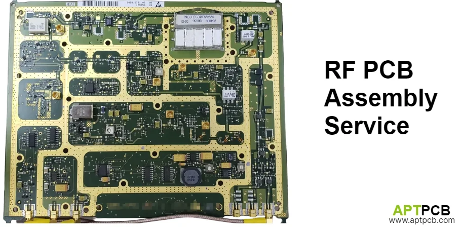
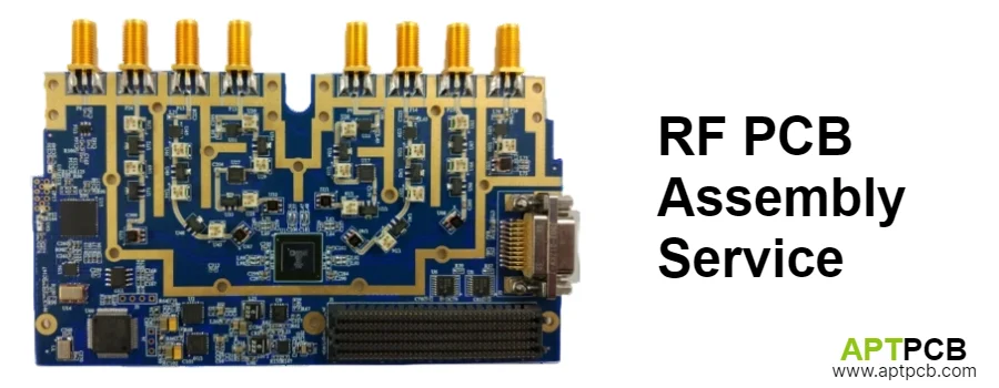
RF PCB assembly transforms bare high-frequency circuit boards into functional radio frequency modules through precision component mounting, specialized soldering processes, and comprehensive testing. Unlike standard electronics assembly where component placement and soldering affect basic functionality, RF assembly requires exceptional precision where component position affects impedance matching, solder joint quality impacts conductor loss, and assembly cleanliness determines long-term reliability.
This guide covers the key aspects of RF PCB assembly—placement accuracy, soldering optimization, sensitivity management, testing requirements, and quality systems—providing engineers with understanding to specify appropriate assembly requirements.
Achieving Precision Component Placement
Component placement accuracy in RF assemblies directly affects circuit performance. RF components require positioning accuracy ensuring proper impedance transitions, minimal parasitic effects, and designed electromagnetic coupling.
Placement Accuracy Requirements
Standard assembly tolerances may be inadequate for demanding RF applications:
Position Tolerance: Typically ±2 mil (±50 μm) or better required for optimal RF performance. Component position affects:
- Trace-to-pad transitions influencing impedance continuity
- Solder fillet geometry impacting high-frequency parasitics
- Alignment with underlying features (thermal vias, ground connections)
Rotation Accuracy: Within ±0.5° to prevent asymmetric solder joints affecting RF performance, particularly for directional components and coupled structures.
Fine-Pitch Component Handling
RF designs increasingly use fine-pitch packages:
QFN/DFN Packages: Common for RF ICs—require accurate placement for proper ground paddle connection and thermal dissipation.
0201/01005 Passives: Tiny components demand precise pick-and-place capability with vision-guided placement.
BGAs: High-density RF devices require accurate placement and reflow for reliable hidden solder joints.
Shield Can Assembly
RF shield cans require accurate placement for effective shielding:
- Perimeter must align with PCB ground pattern
- Incomplete contact creates gaps reducing isolation
- Dense ground via pattern beneath can perimeter essential
Key Placement Accuracy Requirements
- Position Tolerance: Component placement within ±2 mil for proper alignment.
- Rotation Accuracy: Angular alignment within ±0.5° preventing asymmetric joints.
- Fine-Pitch Capability: Equipment handling 0.4mm pitch and smaller.
- Coplanarity Management: Component flatness verification for consistent joints.
- Shield Can Alignment: Accurate positioning for complete perimeter contact.
- Vision System Accuracy: Fiducial recognition for precise placement reference.
Optimizing Soldering Processes for RF Performance
Solder joint quality affects both electrical performance and reliability. Joint geometry influences high-frequency parasitics, void content affects thermal resistance, and intermetallic formation determines mechanical integrity.
Reflow Profile Optimization
RF assemblies require careful profile development:
Material Considerations:
- Some RF laminates have lower thermal tolerance than FR-4
- PTFE materials may require reduced peak temperatures
- Extended time above liquidus can damage temperature-sensitive components
Profile Parameters:
- Preheat rate: 1-3°C/sec typical
- Soak time: 60-120 seconds for thermal equalization
- Peak temperature: 235-250°C for SAC alloys (material-dependent)
- Time above liquidus: 45-90 seconds
Solder Paste Selection
Paste characteristics affecting RF assembly:
- Rheology: Consistent printing on fine-pitch pads
- Slump Resistance: Maintains definition through placement and reflow
- Flux Activity: Adequate for oxide removal without excessive residue
- Voiding Tendency: Low void formation for thermal and RF performance
Selective Soldering
Through-hole RF connectors often require selective soldering:
- Precision systems apply solder to specific locations
- Temperature control prevents damage to adjacent SMT components
- SMA, SMP, and other RF connectors with through-hole pins benefit from selective process
Key Soldering Process Factors
- Profile Optimization: Parameters respecting material and component limits.
- Paste Selection: Appropriate rheology and flux activity for RF applications.
- Void Minimization: Parameters and paste reducing void content.
- Selective Soldering: Precision application for through-hole connectors.
- Nitrogen Atmosphere: Inert reflow improving wetting for fine-pitch components.
- Profile Verification: Thermocouple monitoring through comprehensive assembly processes.
Managing Moisture and Contamination Sensitivity
RF assemblies exhibit sensitivity to moisture and contamination affecting manufacturing success and field reliability.
Moisture Sensitive Device (MSD) Management
Many RF components carry MSD classifications:
Floor Life Tracking:
- Components absorb moisture after removal from dry storage
- Exposure limits (floor life) depend on MSD level
- Level 3 devices: 168 hours at <30°C, <60% RH
- Level 2a: 4 weeks; Level 1: unlimited
Baking Requirements:
- Components exceeding floor life require baking
- Typical: 24-48 hours at 125°C (component-dependent)
- Removes absorbed moisture preventing reflow defects
Board Baking
RF laminates may require pre-assembly baking:
- Moisture in substrates can cause delamination during reflow
- Absorbed moisture affects dielectric properties
- Typical: 2-4 hours at 125°C before assembly
Contamination Control
Contamination affects RF performance and reliability:
Ionic Contamination:
- Can cause electrochemical migration
- May affect high-frequency surface resistance
- Cleaning and verification essential
Flux Residue:
- Some flux residues are conductive at RF frequencies
- No-clean residues must be verified benign
- Critical applications may require cleaning despite "no-clean" designation
Key Sensitivity Management Approaches
- MSD Tracking: Floor life monitoring for moisture-sensitive components.
- Component Baking: Moisture removal for components exceeding exposure limits.
- Board Preparation: Pre-assembly baking for moisture-susceptible laminates.
- Environment Control: Clean assembly areas minimizing contamination.
- Cleaning Processes: Post-assembly cleaning when required for RF performance.
- Coating Protection: Conformal coating for environmental protection.
Implementing Comprehensive RF Testing
RF assembly testing validates both manufacturing quality and RF performance, going beyond standard verification to confirm RF specifications.
In-Process Testing
In-Circuit Testing (ICT) / Flying Probe:
- Verifies component presence and value
- Detects solder opens and shorts
- Catches assembly defects before RF testing
- Automated test systems provide efficient verification
Automated Optical Inspection:
- AOI systems examine solder joints and placement
- Detects insufficient solder, bridging, tombstoning
- Verifies shield can placement and connector seating
X-Ray Inspection:
- Internal examination for BGA and QFN packages
- Void percentage measurement for thermal performance
- Hidden joint verification
RF Functional Testing
RF-specific testing verifies performance:
S-Parameter Measurement:
- Return loss (S11) confirming impedance matching
- Insertion loss (S21) verifying transmission efficiency
- Isolation measurements for multi-port devices
Power Testing:
- Output power for transmitter sections
- Gain and efficiency for amplifiers
- Power handling for passive networks
Frequency Accuracy:
- Synthesizer and oscillator verification
- Filter center frequency and bandwidth
Key RF Testing Requirements
- Electrical Verification: ICT/flying probe confirming component values and connections.
- Visual Inspection: AOI examining joints, placement, shield installation.
- X-Ray: Hidden joint verification for BGA and QFN packages.
- RF Characterization: S-parameters confirming RF specifications.
- Environmental Testing: Temperature cycling for reliability screening.
- Final Inspection: Quality verification before release.
Providing Complete Manufacturing Integration
RF PCB assembly achieves maximum efficiency when integrated with board fabrication, creating seamless flow from design through completed assembly.
Turnkey Assembly Benefits
Turnkey RF assembly combines:
- Board fabrication with appropriate RF materials and tolerances
- Component procurement including specialized RF parts
- Assembly with RF-specific processes
- Testing validating complete RF performance
Single-source responsibility simplifies management and clarifies accountability.
Component Sourcing
Component sourcing addresses RF procurement challenges:
- Long lead times for specialized RF components
- Minimum order quantities exceeding prototype needs
- Counterfeit risk for high-value RF parts
- Supplier relationships ensuring availability
Engineering Support
Technical support throughout manufacturing:
- DFM review identifying assembly challenges before production
- Test strategy development for RF validation
- Process optimization improving yield and quality
- Issue resolution with technical expertise
Key Integration Benefits
- Single-Source Responsibility: Simplified coordination and clear accountability.
- Coordinated Scheduling: Aligned fabrication and assembly reducing lead time.
- Quality Optimization: Process integration enabling end-to-end optimization.
- Component Solutions: Sourcing expertise addressing RF procurement challenges.
- Engineering Partnership: Technical support for DFM and test development.
- Scalable Capacity: Prototype through production capabilities.
Delivering RF Assembly Solutions
RF PCB assembly serves diverse applications across industries:
Telecommunications: Infrastructure equipment including base stations, small cells, and backhaul.
Automotive: Radar systems for ADAS and autonomous driving.
Aerospace: Communication and navigation equipment with stringent reliability requirements.
Consumer: Wireless modules for IoT, WiFi, and Bluetooth applications.
Each application presents specific requirements for RF performance, environmental reliability, and production volume addressed through appropriate assembly processes and quality systems.
For comprehensive manufacturing information, see our guide on high frequency PCB manufacturing.