High frequency PCB manufacturing transforms specialized low-loss materials into precision circuit boards operating from hundreds of MHz through millimeter-wave frequencies. These boards serve critical applications in telecommunications infrastructure, aerospace systems, automotive radar, medical imaging, and wireless devices where signal integrity at elevated frequencies determines system performance. Professional manufacturing requires advanced material handling, precision process control, and comprehensive testing ensuring consistent electrical performance.
This guide covers the essential aspects of high frequency PCB manufacturing—from material selection through final testing—providing engineers with the knowledge needed to specify and obtain boards meeting demanding RF requirements.
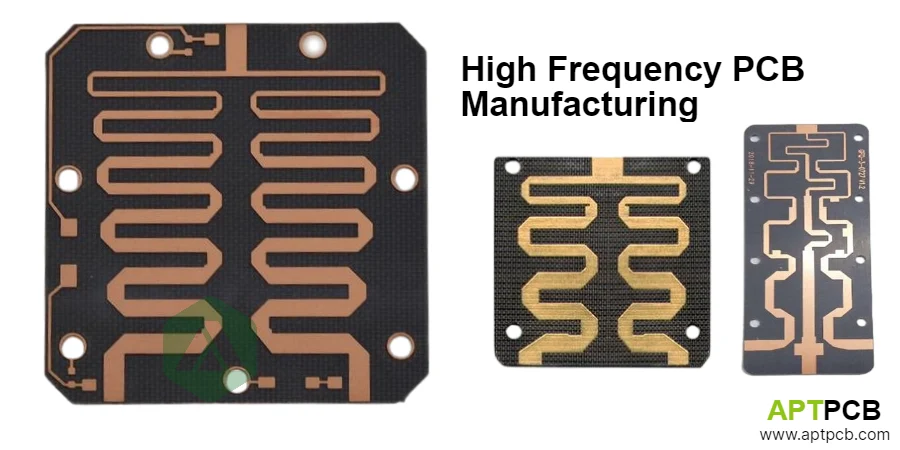
Understanding High Frequency PCB Material Systems
Material selection fundamentally determines high frequency PCB performance. Standard FR-4 exhibits excessive loss and dielectric variation above 1 GHz, requiring specialized laminates with controlled electrical properties. Different material families address specific frequency ranges, thermal requirements, and cost targets.
The dielectric constant (Dk) determines signal propagation velocity and trace impedance relationships—stable Dk values across frequency and temperature ensure predictable circuit behavior. Dissipation factor (Df) represents signal energy lost as heat in the substrate, directly impacting insertion loss that accumulates along trace lengths.
Key Material Selection Criteria
- PTFE-Based Laminates: Rogers RT/duroid series providing loss tangent values below 0.001 for microwave and millimeter-wave applications, though requiring specialized drilling and lamination processes due to soft material characteristics.
- Ceramic-Filled Materials: Rogers RO3000 and similar ceramic-filled PTFE materials offering excellent dielectric stability across -50°C to +150°C temperature ranges for outdoor and aerospace environments.
- Hydrocarbon Ceramics: Rogers RO4000 series providing good high frequency performance with processing characteristics closer to standard FR-4, enabling cost-effective solutions up to approximately 10 GHz.
- Mixed Dielectric Designs: Cost-optimized constructions using premium materials only on critical RF layers combined with standard substrates through multilayer board construction.
- Copper Foil Selection: Low-profile and reverse-treated foils reducing surface roughness and minimizing skin effect losses at elevated frequencies where current flows primarily near conductor surfaces.
- Thermal Considerations: Material selection accounting for thermal expansion matching and temperature stability across operating conditions to ensure long-term reliability.
Material Performance Trade-offs
PTFE materials deliver the lowest electrical losses but present manufacturing challenges—soft material tends to smear during drilling, requires plasma desmear for plating adhesion, and needs modified lamination cycles. Hydrocarbon ceramics process more easily but exhibit higher loss at frequencies above 10 GHz. Understanding these trade-offs enables appropriate material selection balancing performance requirements with manufacturability and cost.
Achieving Precision Impedance Control
Controlled impedance is fundamental to high frequency PCB performance. Transmission lines, matching networks, and interconnects require precise characteristic impedance—typically within ±5% to ±10%—to minimize reflections and maximize power transfer. Achieving consistent impedance across production requires coordinated control of multiple fabrication parameters.
Characteristic impedance depends on trace geometry (width, thickness, distance to reference plane), dielectric constant, and copper characteristics. Manufacturing variations in any parameter directly translate to impedance variations. For example, a 1 mil change in trace width on a 50Ω microstrip line can shift impedance by approximately 2-3Ω.
Key Impedance Control Techniques
- Trace Geometry Management: Photolithography and etching processes maintaining trace width tolerance within ±0.5 mil through optimized exposure parameters, consistent resist thickness, and controlled etch chemistry with documented compensation factors.
- Dielectric Thickness Control: Lamination processes controlling prepreg flow and final dielectric thickness within ±10% of nominal values, accounting for copper density variations across the panel that affect prepreg compression.
- Copper Weight Uniformity: Plating processes delivering consistent copper thickness across panel areas without excessive center-to-edge variation, critical for both impedance accuracy and current carrying capacity.
- Test Coupon Verification: Every production panel includes impedance test coupons with TDR (Time Domain Reflectometry) measurement validating achieved values match design targets.
- Statistical Monitoring: Process capability analysis tracking Cpk values for critical parameters ensures consistent impedance delivery across production lots, enabling early detection of process drift.
- Stack-Up Modeling: Pre-production impedance modeling using field solver tools, validated against actual manufacturing results, confirms designed impedance values are achievable with specified tolerances.
For more information on impedance requirements, see our guide on controlled impedance high frequency PCB.
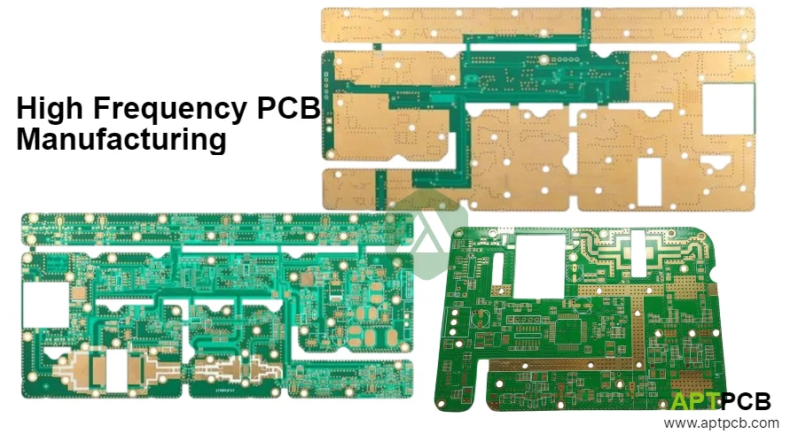
Implementing Advanced Via Structures
Via structures significantly impact high frequency performance through inductance, capacitance, and potential resonances. A standard 10-mil through-hole via exhibits approximately 0.5-1 nH inductance—negligible at low frequencies but significant at GHz operation where this inductance creates impedance discontinuities affecting signal integrity.
The most critical high-frequency via issue is stub resonance. When a signal transitions from one layer to another through a via, the unused portion of the via barrel acts as a transmission line stub. This stub resonates at frequencies where its electrical length equals a quarter wavelength, creating a notch in signal transmission that can fall within the operating bandwidth.
Key Via Technology Capabilities
- Controlled-Depth Back Drilling: Removing unused via barrel portions eliminates stub resonances. Depth control accuracy within ±4 mils ensures complete stub removal without damaging internal layer connections. A 40-mil stub removed through back drilling shifts resonance from approximately 10 GHz to well above operating frequencies.
- Laser-Drilled Microvias: Precision laser drilling enables microvia diameters below 100 μm, minimizing parasitic inductance in dense layouts where standard mechanical drilling cannot achieve required hole sizes.
- Via-in-Pad Technology: Filled and planarized vias directly beneath component pads reduce interconnect length and inductance for high frequency ICs, particularly important for QFN and BGA packages with tight pin spacing.
- Ground Via Fencing: Electromagnetic barriers using via rows with spacing below λ/10 at operating frequency prevent coupling between RF sections. For 10 GHz operation, this means via spacing of approximately 1mm or less.
- Blind and Buried Vias: Layer-specific connections eliminating through-hole stubs, though adding manufacturing complexity and cost requiring sequential lamination processes.
- Aspect Ratio Management: Via diameter must match board thickness to ensure reliable plating—typical aspect ratios of 8:1 to 10:1 for standard processes, with higher ratios requiring specialized plating approaches.
For detailed information on HDI structures, see our HDI circuit board capabilities.
Managing Thermal Requirements
High frequency circuits often dissipate significant power in amplifiers, oscillators, and power conversion stages. A typical RF power amplifier may operate at 40-50% efficiency, meaning half the input power becomes heat that must be removed to maintain junction temperatures within safe operating ranges.
Thermal management becomes particularly challenging when high-power devices mount on low-thermal-conductivity PTFE substrates. Standard PTFE materials exhibit thermal conductivity around 0.2 W/m·K compared to FR-4's 0.3 W/m·K—both significantly lower than metals used for heat spreading.
Key Thermal Management Approaches
- Thermal Via Arrays: Dense via patterns beneath power components transfer heat to internal copper planes or opposite-side spreaders. Typical arrays use 0.3mm diameter vias on 0.6mm pitch, achieving thermal resistance reduction of 50% or more compared to substrate alone.
- Heavy Copper Layers: 2-4 oz copper weight serves dual functions as current carriers and heat spreaders in power sections. The increased copper mass significantly improves lateral heat spreading from concentrated sources. See our heavy copper construction capabilities.
- Metal Core Integration: Aluminum or copper core boards provide direct thermal paths for high-power RF stages, achieving thermal conductivity improvements of 100x over standard substrates.
- Copper Coin Embedding: Solid copper inserts beneath critical components provide enhanced thermal conductivity paths while maintaining the RF performance of surrounding low-loss substrate materials.
- Interface Provisions: Board features accommodating thermal interface materials and heatsink attachment, including appropriate surface finishes and dimensional tolerances for thermal compound application.
- Thermal Modeling: Design analysis using finite element methods predicts temperature distributions before fabrication, enabling optimization of via patterns and copper placement.
Ensuring Environmental Reliability
High frequency PCBs often operate in demanding environments requiring robust construction and environmental protection. Telecommunications equipment faces temperature cycling from -40°C to +85°C, automotive radar experiences vibration and thermal shock, and aerospace systems must survive altitude pressure changes and extended temperature ranges.
Material stability across temperature is critical—the dielectric constant of some materials changes by several percent across a 100°C temperature range, causing corresponding impedance shifts that can move circuits out of specification.
Key Environmental Protection Methods
- Material Stability: Glass transition temperatures (Tg) above 170°C prevent property changes during lead-free assembly peak temperatures and high-temperature operation. Materials with Tg below operating temperature exhibit dramatically different mechanical and electrical properties.
- Moisture Resistance: Low moisture absorption materials (typically below 0.1% by weight) prevent dielectric constant shifts in humid environments. PTFE materials inherently exhibit very low moisture absorption, while other laminates require careful specification.
- Conformal Coating: Protective coating application protecting assemblies from moisture, contamination, and handling damage, particularly important for assemblies operating in condensing humidity or marine environments.
- Temperature Range: Component and material selection supporting operation from -40°C to +85°C (commercial) or -55°C to +125°C (military grade), with attention to coefficient of thermal expansion matching between materials.
- Vibration Resistance: Construction methods withstanding mechanical stress in mobile and aerospace applications, including appropriate component attachment techniques and board mounting provisions.
- Outgassing Control: Material selection meeting NASA ASTM E595 requirements for space applications where outgassed materials can contaminate optical surfaces or create conductive paths.
For high temperature stability, see our high-Tg laminate selection guide.
Comprehensive Testing and Quality Assurance
High frequency PCB manufacturing requires testing beyond standard electrical verification. Material properties, impedance accuracy, and dimensional precision must all be validated to ensure boards perform as designed in demanding RF applications.
Testing costs increase with frequency—while simple TDR impedance measurement suffices for many applications, millimeter-wave circuits may require vector network analysis through 67 GHz or higher, using specialized fixtures and calibration procedures.
Key Testing Capabilities
- Impedance Testing: TDR measurement on production panels verifies controlled impedance traces meet specifications. Test results provide both pass/fail determination and diagnostic information identifying process variations.
- Dimensional Verification: Precision measurement confirming trace widths (typically ±0.5 mil tolerance), spacing, and registration meet design requirements. Automated optical inspection supplements manual measurement for complete coverage.
- Material Traceability: Complete certification and lot traceability supporting quality requirements for aerospace, defense, and medical applications where material origin documentation is mandatory.
- Electrical Testing: Automated probe testing verifying connectivity and isolation on complex boards, detecting opens, shorts, and incorrect component values.
- Visual Inspection: Automated optical inspection detecting defects affecting performance including trace damage, contamination, and plating anomalies.
- Cross-Section Analysis: Microsection examination validating plating quality, layer registration, and via structure for process qualification and lot sampling.
Quality systems meeting PCB quality standards ensure consistent results across production volumes.
Supporting Complete Product Development
High frequency PCB manufacturing serves diverse development stages from prototypes requiring rapid iteration through high-volume production demanding consistent quality and competitive cost.
Key Production Capabilities
- Prototype Development: Rapid prototype services enable design iteration with quick-turn delivery while maintaining quality standards—critical for development programs where schedule pressure is intense.
- Production Manufacturing: Volume production delivers consistent quality across extended production runs with statistical process control ensuring part-to-part repeatability.
- Assembly Integration: Complete turnkey services combining fabrication with precision component mounting eliminates supplier coordination complexity for complete RF assemblies.
- Engineering Support: DFM review and optimization recommendations improve manufacturability before production commitment, reducing iterations and accelerating time to market.
- Material Management: Supplier relationships ensure availability of specialized high frequency laminates, managing the longer lead times typical of premium RF materials.
- Industry Applications: Proven capabilities across telecommunications infrastructure and automotive radar applications demonstrate real-world performance in demanding environments.
Through material expertise, precision processes, and responsive engineering support, capable high frequency PCB manufacturing enables successful RF, microwave, and high-speed programs across the full range of applications.