- Controlled impedance high frequency PCB work should be treated as a path-sensitive RF release problem, not as a generic promise that a board uses premium laminate and therefore must perform well.
- The most useful review boundary is simple: first decide which RF or loss-sensitive board paths are truly critical, then review structure type, material scope, local transitions, and layered validation in that order.
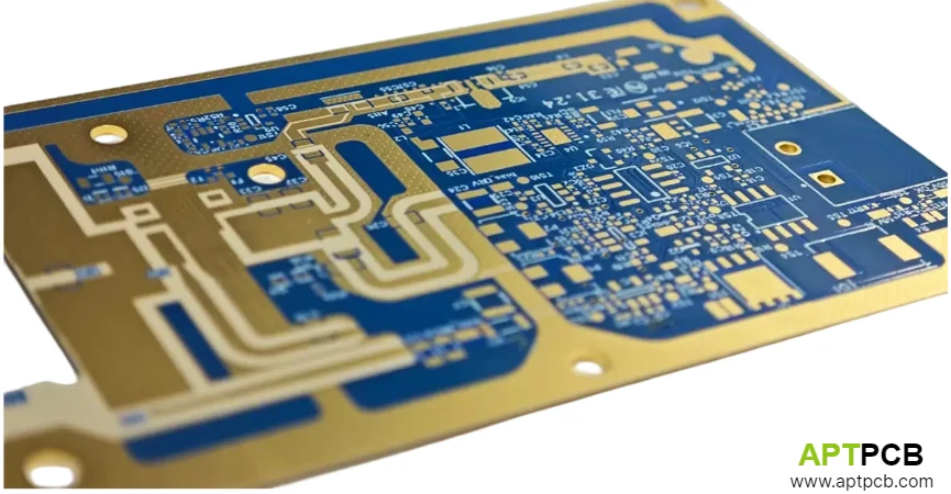
- A board can mention
50 ohm,low loss, orRF materialand still release weakly if the path boundary, launch cleanup, or validation ownership is vague. - Release claims should stay at the fabricated-board path boundary, while VNA, chamber, and full product validation remain later-stage evidence.
Quick Answer
A controlled impedance high frequency PCB is a board where selected RF-sensitive paths are released as measurable transmission structures rather than generic traces. The engineering decision is which part of the RF path actually needs controlled structure, which material family fits that path, and what evidence still has to come later before the whole application can be treated as proven.
For the broader view that connects high-speed and RF board release, start with the High-Speed and RF PCB Manufacturing Guide.
Table of Contents
- What should engineers review first?
- What does controlled impedance high frequency PCB mean here?
- Why RF path scope and material family come before exact claims
- Why transitions and reference continuity still decide the board outcome
- What this board class does not prove by itself
- What should be frozen before release?
- Next steps with APTPCB
- FAQ
- Public references
- Author and review information
What should engineers review first?
Start with these five boundaries:
- RF path ownership
- structure type and material scope
- transition and return continuity
- fabrication correlation
- later validation ownership
That order matters because RF board work is often overstated through material names alone. The stronger engineering question is narrower:
Which parts of the board path are truly RF-sensitive enough that they need a controlled structure, and which parts are only adjacent support context?
The first questions are usually:
- Which lines are really carrying the high-frequency burden?
- Is the board using the right transmission-line family for the intended path?
- Does the design justify premium RF laminate everywhere, or only on selective layers or regions?
- Are the risky failures more likely to appear at launches, vias, shielding edges, or reference interruptions?
- Is the claim expanding from board-level evidence into full RF-system proof?
| Review boundary | What it answers | What it does not prove |
|---|---|---|
| RF path ownership | Which board paths truly need controlled RF treatment | Whole-product wireless or compliance performance |
| Structure type and material scope | Whether the physical route matches the path burden | That every region needs the same laminate strategy |
| Transition and return continuity | Whether local discontinuities are being handled before release | Final insertion-loss, OTA, or field results |
| Fabrication correlation | Whether the structure can be reviewed against board-level intent | Full platform validation in every environment |
| Later validation ownership | Which evidence still belongs outside the fabricated board | That the board alone replaces RF-system testing |
What does controlled impedance high frequency PCB mean here?
Here, controlled impedance high frequency PCB means a board where selected RF-sensitive paths are released as measurable transmission structures with explicit material and validation posture.
That usually includes:
- microstrip, stripline, or related RF transmission-line structures
- board regions where low-loss material scope matters
- launch and via transitions that can consume margin early
- coupon or comparable board-level correlation posture
- a clean boundary between fabrication evidence and later RF measurements
It does not automatically mean:
- that every copper feature on the board is RF-critical
- that any one laminate family is universally correct
- that coupon or TDR evidence proves the whole RF application
- that chamber, antenna, or product-level behavior is already resolved
This scope stays at the board execution boundary and does not extend to full wireless-device proof.
Why RF path scope and material family come before exact claims
High-frequency board claims become weak when premium RF laminate is treated as proof of path performance.
The review questions are:
- Which layers or regions actually carry the RF burden?
- Does the board need a full RF laminate route or a hybrid stackup strategy?
- Is the material choice tied to real path sensitivity rather than branding?
- Are structure and laminate decisions being reviewed together with transition posture?
| Material question | Why it matters | Common mistake |
|---|---|---|
| Which path is truly RF-sensitive? | Material scope should follow the real burden | Premium laminate is named too broadly |
| Is hybrid scope justified? | Hybrid builds often balance performance and manufacturability better | A full premium stack is implied without path logic |
| Is structure choice clear? | Microstrip, stripline, or related structures change the board posture | Geometry language stays vague while claims get stronger |
| Is material choice tied to later validation? | Material naming alone does not prove the RF path works | Laminate identity is treated like end proof |
For material and transmission-line route planning, review High Frequency PCB, RF Rogers Materials, and Megtron PCB before making broad capability claims.
Why transitions and reference continuity still decide the board outcome
In high-frequency work, local discontinuities often consume margin before long-path theory becomes the main problem.
That includes:
- connector launches
- probe or feed transitions
- via changes between RF layers
- ground-via cleanup near signal vias
- reference interruptions around shielding or copper voids
- hybrid-stackup region changes
| Transition area | Why it matters | What usually goes wrong |
|---|---|---|
| Launch geometry | The path can lose performance at the entry point | Launches are left generic while claims get stronger |
| Via transitions | Local discontinuities shape the effective RF path | Vias are treated as neutral instead of sensitive events |
| Reference continuity | Return current and field shape are part of the same structure | Plane or ground behavior is ignored while only traces are reviewed |
| Hybrid region changes | Material transitions can change manufacturability and path posture | Mixed-material execution is described too loosely |
A common high-frequency failure chain starts when a launch, via transition, or hybrid-material boundary is left vague while the article still assumes the RF path is under control. The fabricated board then carries a discontinuity in field shape or return continuity, the path sees mismatch or excess loss earlier than expected, and coupon, TDR, or later RF measurement has to uncover a board-level problem that should have been frozen before release. Instead of validating one clear transmission structure, the team is debugging mixed-material transitions, launch cleanup, or reference handling after the board already claimed a stronger RF posture.
The harsher microwave version appears when a team spends serious money on surface RF laminate such as RO4350B for a 28 GHz 5G millimeter-wave board or a 77 GHz automotive radar front end, then treats the connector launch and layer transition as routine PCB details. The RF energy enters through an SMA launch, drops through a via into an inner-layer path, and the fabrication drawing never locked two critical controls: backdrill depth and dense ground Stitching Vias around the transition. At these frequencies, even a 10 mil via stub is no longer a harmless leftover conductor. It becomes a destructive Via Stub Resonance structure, effectively an open-ended resonant element. The result is not subtle. Energy that should have remained in the intended line falls into a deep Insertion Loss Dip, often -10 dB or worse at the target band. At the same time, the missing reference cage lets the leaking field radiate into nearby digital-ground cavities, so the transition starts behaving like a Radiating Antenna instead of a clean RF handoff. The path that was supposed to feed the radar or millimeter-wave front end ends up blinding the receiver with its own leaked energy. That is how a board built from premium RF laminate turns into an expensive radiator when transition discipline is weak.
The governing rule is:
if the local RF transition is still vague, the release package overstates the board's RF readiness.
What this board class does not prove by itself
One of the most common RF content failures is collapsing all evidence into one statement like the board passed testing.
That is too broad.
| Evidence layer | What it supports | What it does not prove |
|---|---|---|
| Board-level structure and material review | The RF-sensitive path is being released with intent | Full RF system performance |
| Coupon or TDR-style board correlation | The fabricated structure matches the intended board-level posture | Whole-channel, antenna, or chamber behavior |
| Deeper RF measurements | Specific RF-path evidence in scope | That every product environment is already covered |
| Product or platform validation | Real end-use proof in the final configuration | That the board alone was sufficient |
That boundary matters because:
- controlled impedance is not the same thing as RF proof
- low-loss material is not the same thing as system proof
- a board-level measurement posture is not chamber or OTA proof
What should be frozen before release?
Before this board class is released responsibly, freeze:
- the RF-sensitive path scope
- the structure type and layer ownership
- the material scope for the path that truly needs it
- the transition and reference-cleanup posture
- the boundary between board-level correlation and later RF validation
If those items are still moving, the board may still be a useful engineering draft, but it should not be framed as a stable controlled-impedance high-frequency release.
Next steps with APTPCB
If your high-frequency board is already losing margin at connector launches, mixed-material transitions, or suspicious via events, and you suspect that Via stubs are quietly consuming the RF link budget, do not let premium laminate names hide a weak transition structure. At microwave frequency, the failure usually starts where the path changes shape, not where the laminate marketing sounds strongest.
Send the Gerber or ODB++ package, backdrill requirements, hybrid stackup intent, and target frequency band to sales@aptpcb.com or through the quote page.
APTPCB's high-frequency CAM and microwave engineering team will return an RF Transition & Hybrid Structure Review within 24 hours. We will identify launch-area impedance discontinuity, verify backdrill and reference-continuity assumptions, and expose the transition defects most likely to waste expensive RF laminate before you spend serious money on blind prototype iteration.
Useful related reading:
FAQ
Does controlled impedance high frequency PCB mean the whole board uses premium RF laminate?
No. The right material scope depends on which paths actually carry the RF burden.
Does a board-level impedance posture prove RF system performance?
No. It supports fabricated-board release discipline, not the full RF application outcome.
Is hybrid material strategy a compromise?
Not by default. It can be the correct posture when only selected layers or regions carry the real RF burden.
What usually breaks first?
Launches, vias, return-path discontinuities, and vague mixed-material transitions often consume margin early.
Should this kind of page claim OTA or compliance proof?
No. Those claims sit outside the safe board-level evidence boundary.
Public references
High-Speed and RF PCB Manufacturing Guide Broader guide for high-speed and RF board-release discipline.
Cadence RF PCB Design Guidelines Supports RF transmission-line structure planning, launch discipline, and high-frequency layout boundaries.
Ansys: Coplanar Waveguide Driven Terminal Supports structure-identity language for RF transmission-line families without turning topology names into outcome proof.
High Frequency PCB Support-page context for RF-sensitive fabrication and stackup planning.
RF Rogers Materials Support-page context for RF laminate-family selection.
Author and review information
- Author: APTPCB RF structure and validation content team
- Technical review: RF stackup, transition, and measurement-planning engineering team
- Last updated: 2026-05-15