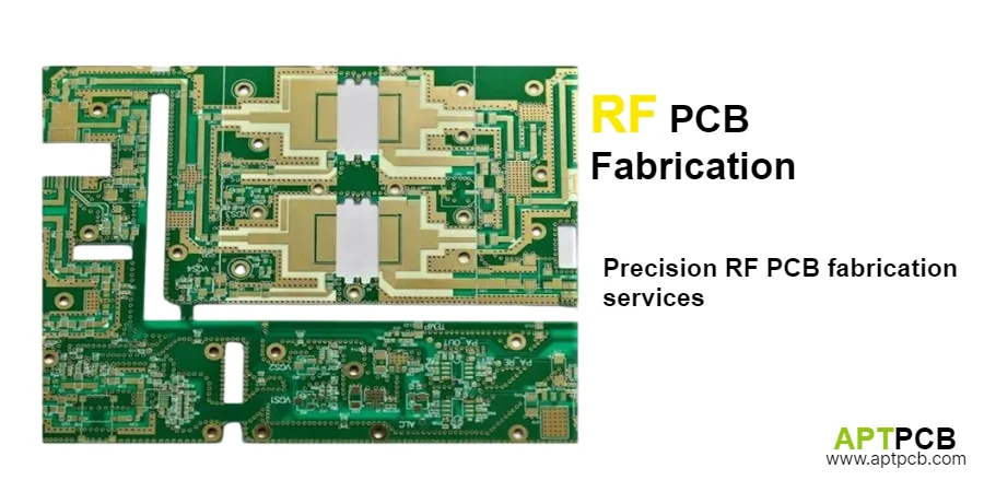
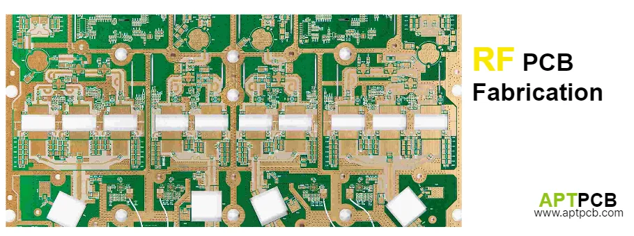
RF PCB fabrication transforms specialized high-frequency materials into precision circuit boards through carefully controlled manufacturing processes that differ significantly from standard PCB production. Unlike conventional fabrication where materials behave predictably and tolerances accommodate variation, RF fabrication requires modified procedures for processing soft PTFE materials, maintaining tight impedance tolerances, achieving dimensional accuracy within thousandths of an inch, and validating RF-specific parameters.
This guide examines the key RF PCB fabrication processes—material handling, impedance control, drilling, plating, surface finish, and testing—providing engineers with understanding to create manufacturable designs and specify appropriate requirements.
Processing Specialized RF Laminate Materials
RF laminates—PTFE composites, ceramic-filled materials, hydrocarbon ceramics—exhibit different physical and chemical characteristics than standard FR-4, requiring modified fabrication processes throughout manufacturing.
PTFE Material Challenges
PTFE-based materials present specific manufacturing challenges:
Drilling: The soft, thermoplastic nature causes material to smear across hole walls during mechanical drilling. This smear can block subsequent copper plating, creating unreliable via connections. Solutions include:
- Reduced spindle speeds (typically 40-60% of FR-4 parameters)
- Optimized feed rates balancing chip evacuation with smear prevention
- Specialized drill geometries with increased relief angles
- Plasma desmear processing removing residual smear after drilling
Surface Preparation: PTFE's low surface energy (18-20 dynes/cm vs 40-50 for epoxy) resists copper adhesion. Surface treatments include:
- Sodium naphthalenide etching (chemical modification of surface)
- Plasma treatment (physical roughening and chemical activation)
- Specialized adhesion promoters
Ceramic-Filled Materials
Ceramic-filled laminates contain abrasive particles causing rapid tool wear:
- Drill life may decrease 50-80% compared to standard materials
- More frequent tool changes required (typically every 1000-2000 hits vs 3000-5000)
- Specialized carbide or diamond-coated tools extend life but increase cost
Lamination Considerations
RF materials require adapted lamination parameters:
- PTFE materials exhibit unique flow characteristics—typically less flow than epoxy systems
- Extended dwell times may be required for complete cure
- Hybrid constructions combining RF and standard materials need compatible bonding through specialized manufacturing techniques
Key Material Processing Requirements
- Drill Parameter Optimization: Speed, feed, and tool geometry preventing smearing while maintaining hole quality.
- Desmear Processing: Plasma or chemical treatment ensuring clean hole walls for plating.
- Tool Management: Frequent changes and wear monitoring maintaining consistent quality.
- Lamination Profiles: Material-specific temperature, pressure, and time cycles.
- Surface Preparation: Treatments enabling reliable copper adhesion.
Achieving Precision Impedance Control
Controlled impedance—typically ±5% or ±10% tolerance—is fundamental to RF PCB performance. Achieving consistent impedance requires maintaining trace width, dielectric thickness, and copper weight within tight tolerances throughout fabrication.
Trace Width Control
Trace width is the primary impedance variable within a given stackup. The fabrication process chain includes:
Photolithography:
- Exposure energy optimization—under-exposure causes resist lifting, over-exposure causes line spread
- Resist thickness uniformity affecting sidewall profile
- Development parameters controlling resist removal
Etching:
- Etch rate uniformity across panel area
- Undercut control—copper etches laterally beneath resist creating trapezoidal cross-section
- Etch factor documentation enabling compensation (typically +0.3 to +0.7 mil per side)
Combined processes must achieve trace width tolerance within ±0.5 mil for ±5% impedance control.
Dielectric Thickness Control
Dielectric thickness between trace and reference plane directly affects impedance (approximately 0.5Ω per mil thickness change for typical 50Ω microstrip).
Lamination parameters affecting thickness:
- Prepreg resin content and flow characteristics
- Press temperature and pressure profiles
- Copper density variations affecting local flow
Manufacturing must control these parameters achieving thickness within ±10% of design values.
Test Coupon Verification
Every production panel should include impedance test coupons:
- Coupon structures matching actual board geometries
- TDR measurement validating achieved impedance
- Statistical tracking through rigorous quality systems
Implementing Precision Drilling and Via Formation
Via structures in RF circuits require precise positioning, quality hole walls, and appropriate diameter to support controlled impedance transitions.
Mechanical Drilling
Standard mechanical drilling remains the primary method for through-hole vias:
- Position accuracy typically ±2 mil required for proper feature connection
- Clean hole walls without burrs enable reliable plating
- Aspect ratio limits (typically 8:1 to 10:1) constrain diameter vs thickness
Controlled-Depth Drilling
Back-drilling removes via stubs that create quarter-wave resonances:
- Depth control accuracy typically ±4 mils
- Allows 4-6 mil margin from active layer
- Adds approximately 10-15% to fabrication cost
Laser drilling creates microvias below 100 μm diameter for HDI structures.
Achieving RF-Grade Copper Quality
Copper plating affects impedance, thermal performance, and high-frequency losses. At microwave frequencies, current flows in the surface skin layer making surface characteristics critical.
Surface Roughness
Copper surface roughness directly impacts skin effect losses:
- At 10 GHz, skin depth in copper ≈ 0.66 μm
- Standard electroplated copper: Rz ≈ 3-7 μm
- Smooth copper: Rz ≈ 1-2 μm
- Loss improvement of 10-20% possible with smooth copper at 10+ GHz
Thickness Uniformity
Plating thickness variation affects impedance—target uniformity ±10% of nominal thickness across panel area.
Managing Surface Finish for RF Applications
Surface finish affects RF performance and must provide solderability and appropriate shelf life.
Finish Options
ENIG: Excellent solderability but nickel layer may cause losses at high frequencies (0.1-0.3 dB at 10 GHz).
Immersion Silver: Excellent RF performance, good solderability, but 6-12 month shelf life.
OSP: Minimal impedance impact, lowest cost, but limited shelf life (3-6 months).
Key Surface Finish Considerations
- RF performance vs frequency requirements
- Assembly process compatibility through SMT assembly
- Shelf life and storage conditions
- Cost relative to performance benefits
Ensuring Quality Through RF-Specific Testing
RF PCB fabrication requires testing beyond standard verification.
TDR Impedance Testing
Time Domain Reflectometry measures impedance along transmission lines:
- Identifies both impedance value and discontinuity locations
- Test coupons enable non-destructive production verification
Dimensional Inspection
Critical dimensions directly affect RF performance:
- Trace width with ±0.25 mil resolution
- Gap dimensions for coupled structures
- Layer registration verification
Key Testing Requirements
- Impedance Verification: TDR measurement confirming specifications
- Dimensional Inspection: Trace geometry validation
- Material Traceability: Documentation linking boards to material properties
- Electrical Testing: Through automated test systems
Supporting RF Product Development
RF PCB fabrication serves prototypes through production with NPI capabilities for development and volume manufacturing for production.
For comprehensive information, see our guide on high frequency PCB manufacturing.