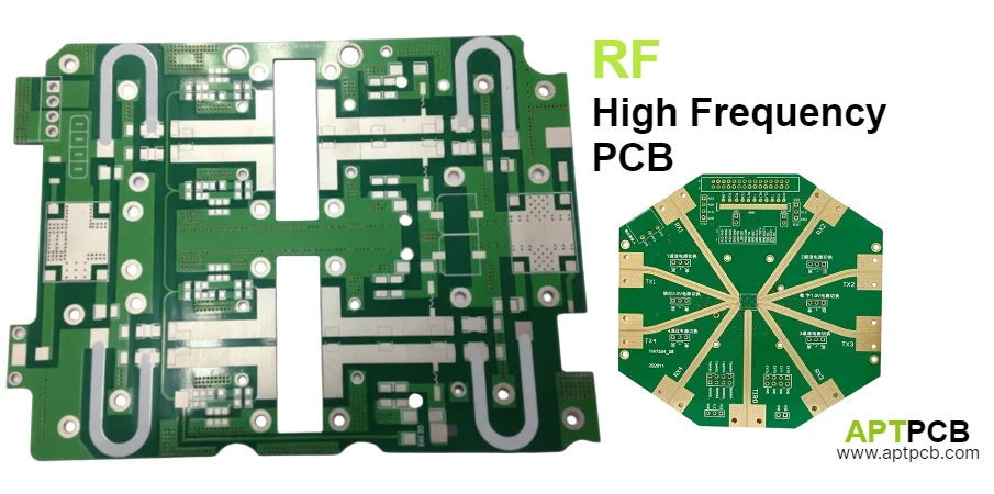
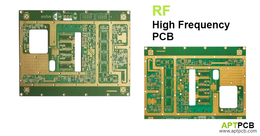
RF high frequency printed circuit boards serve as the critical foundation for modern wireless communication systems, radar applications, satellite infrastructure, and advanced electronic equipment operating across the radio frequency spectrum from hundreds of megahertz to tens of gigahertz. These specialized circuit boards demand precise electrical characteristics including controlled impedance, minimal signal loss, and consistent phase stability requiring advanced materials like PTFE substrates, precision high frequency PCB fabrication processes, and comprehensive testing protocols ensuring reliable signal transmission across demanding frequency ranges.
At APTPCB, we manufacture RF high frequency PCBs with specialized expertise implementing low-loss materials, precision impedance control, and rigorous quality systems. Our capabilities support L-band GPS receivers through Ka-band satellite terminals with validated manufacturing processes from our high frequency PCB manufacturer facilities ensuring performance and reliability.
Achieving Precise Frequency Band Performance
Different RF frequency bands impose distinct requirements on PCB design, material selection, and manufacturing tolerances affecting wireless system performance, radar detection capability, and satellite link budgets. Operating across L-band through Ka-band frequencies requires understanding each band's unique challenges for substrate selection, transmission line design, and loss management. Inadequate frequency-specific optimization causes excessive insertion loss reducing communication range, impedance variations degrading return loss and VSWR, or phase instability affecting beam-forming arrays — directly impacting system performance and operational reliability.
At APTPCB, our manufacturing implements frequency-optimized processes achieving band-specific performance targets.
Key Frequency Band Capabilities
- L-Band (1-2 GHz): GPS receivers, mobile communications, and telemetry systems utilizing Rogers RO4003C substrates achieving insertion loss below 0.5 dB/inch with ±5% impedance tolerance supporting aerospace defense navigation applications.
- S-Band (2-4 GHz): Weather radar, surface ship radar, and satellite uplinks implementing hybrid PTFE/FR-4 constructions balancing performance with cost through RF circuit board manufacturing expertise.
- C-Band (4-8 GHz): Satellite communications and wireless backhaul requiring Rogers RT/duroid 5880 with loss tangent below 0.0009 ensuring minimal signal degradation across extended transmission paths.
- X-Band (8-12 GHz): Military radar and satellite communications demanding ceramic-filled PTFE substrates with tight dielectric constant tolerance (±2%) for precision phase control in phased array modules.
- Ku/K/Ka-Band (12-40 GHz): 5G infrastructure, automotive radar, and high-capacity satellite systems requiring low-loss high frequency PCB materials with smooth copper and precision etching achieving millimeter-wave performance.
Validated Frequency Performance
By implementing frequency-specific material selection, optimized transmission line designs, and band-appropriate manufacturing tolerances supported by comprehensive RF testing, APTPCB enables RF high frequency PCBs achieving target specifications across L-band through Ka-band applications supporting communications, radar, and satellite systems worldwide.
Managing Critical Material Selection Requirements
RF high frequency PCB materials must balance electrical performance, thermal management, mechanical stability, and manufacturing processability with cost considerations varying by application requirements. Selecting appropriate substrates considering dielectric constant, loss tangent, thermal conductivity, and coefficient of thermal expansion determines ultimate circuit performance. Inadequate material selection causes excessive signal attenuation limiting range, dielectric constant variations affecting impedance accuracy, or CTE mismatches causing reliability failures — significantly impacting system performance and long-term reliability.
At APTPCB, our engineering implements comprehensive material selection ensuring application-appropriate performance.
Key Material Technologies
- PTFE-Based Substrates: Rogers RT/duroid, Taconic TLY, and similar glass-reinforced PTFE materials offering loss tangents below 0.001 for demanding microwave RF PCB applications requiring minimum insertion loss.
- Ceramic-Filled PTFE: Rogers RO3000 series combining low loss with enhanced thermal conductivity (0.5+ W/m·K) supporting power amplifier applications with integrated thermal management.
- Advanced Hydrocarbon Laminates: Rogers RO4000 series and Isola Astra providing loss tangents around 0.003-0.004 with FR-4-like processability reducing manufacturing complexity for applications through 10 GHz.
- Ceramic Substrates: Alumina and aluminum nitride for highest frequency applications demanding exceptional dimensional stability, thermal conductivity, and dielectric properties through RF microwave PCB capabilities.
- Hybrid Constructions: Mixed-dielectric stackups combining high-performance materials on RF layers with cost-effective materials elsewhere optimizing performance-to-cost ratio.
- Material Characterization: Incoming inspection verifying dielectric constant and loss tangent ensuring material properties meet specifications through testing quality protocols.
Material Performance Assurance
Through comprehensive material expertise, application-specific selection guidance, and validated processing parameters supported by material characterization capabilities, APTPCB enables RF high frequency PCBs achieving target electrical performance while meeting thermal, mechanical, and economic requirements across diverse applications.
Implementing Precision Transmission Line Design
RF transmission lines must maintain consistent characteristic impedance, minimize losses, and control coupling between adjacent circuits across the operating frequency range. Microstrip, stripline, and coplanar waveguide configurations each offer distinct advantages for specific applications requiring careful selection and optimization. Inadequate transmission line design causes impedance mismatches creating reflections and standing waves, excessive insertion loss degrading signal-to-noise ratio, or crosstalk between circuits causing interference — directly impacting RF system performance and signal integrity.
At APTPCB, our manufacturing implements precision transmission line fabrication achieving demanding impedance and loss specifications.
Key Transmission Line Configurations
- Microstrip Design: Conductor traces over ground plane enabling component access while requiring precise trace width control achieving ±5% impedance tolerance with width tolerances to ±0.5 mil through advanced controlled impedance high frequency PCB processes.
- Stripline Configuration: Signal conductors between ground planes eliminating radiation loss and providing superior isolation for sensitive receiver circuits and high frequency multilayer PCB applications.
- Coplanar Waveguide: Ground-signal-ground structures on single surfaces enabling direct probing, simplified grounding, and flip-chip device integration for MMIC applications.
- Coupled Differential Pairs: Edge-coupled or broadside-coupled differential transmission lines maintaining consistent differential impedance (typically 100Ω) for high-speed digital and balanced RF circuits.
- Via Transition Optimization: Anti-pad sizing, via diameter selection, and ground via placement minimizing transition discontinuities from microstrip to stripline layers.
- Backdrilling Implementation: Controlled-depth drilling removing via stubs preventing resonances at high frequencies through precision depth control capabilities.
Transmission Line Excellence
By implementing precision etching, accurate dielectric control, and optimized via transitions coordinated with field solver analysis and TDR verification, APTPCB enables RF transmission lines achieving impedance tolerances to ±5% with minimized insertion loss supporting demanding high frequency applications.
Ensuring Thermal Management for RF Power Applications
RF power amplifiers, transmit modules, and high-power switching circuits generate significant heat requiring effective thermal management preventing component overheating and performance degradation. Managing thermal paths from power devices through PCB structures to heat sinks determines operational reliability and continuous power handling capability. Inadequate thermal design causes device junction temperatures exceeding ratings reducing reliability, gain compression from thermal effects limiting output power, or thermal runaway in paralleled devices — directly impacting RF system power capability and operational safety.
At APTPCB, our manufacturing implements effective thermal management strategies ensuring reliable high-power operation.
Key Thermal Management Techniques
- Thermal Via Arrays: Dense via patterns (typically 0.3mm diameter on 0.6mm pitch) beneath power devices transferring heat to opposite-side ground planes or heat sink interfaces with thermal resistance below 10°C/W.
- Heavy Copper Construction: 2-4 oz copper in power distribution layers improving lateral heat spreading while handling high DC currents feeding RF power stages.
- Metal Core Integration: Aluminum or copper core substrates providing direct thermal paths from power devices achieving thermal conductivity exceeding 200 W/m·K for high-power high frequency PCB assembly applications.
- Ceramic-Filled Substrates: PTFE materials with ceramic fillers increasing thermal conductivity to 0.5+ W/m·K compared to 0.2 W/m·K for standard PTFE while maintaining low RF losses.
- Component Placement Optimization: Strategic positioning of heat-generating devices avoiding thermal coupling between stages and enabling efficient heat spreading across board area.
- Thermal Simulation Validation: Finite element thermal analysis predicting junction temperatures under worst-case operating conditions validating design before fabrication.
Thermal Performance Validation
Through comprehensive thermal design, validated heat dissipation techniques, and thermal testing under RF operating conditions coordinated with manufacturing processes, APTPCB enables RF high frequency PCBs maintaining safe operating temperatures supporting continuous high-power operation across communications and radar applications.
Controlling EMI/EMC for RF System Integration
RF circuits must coexist with digital control, power management, and other RF subsystems without mutual interference affecting system performance. Managing electromagnetic coupling through shielding, grounding, and layout practices ensures reliable operation meeting regulatory EMC requirements. Inadequate EMI control causes receiver desensitization from local oscillator leakage, digital noise contaminating sensitive RF circuits, or spurious emissions violating regulatory limits — significantly impacting system performance and certification compliance.
At APTPCB, our manufacturing implements comprehensive EMI control strategies ensuring RF system compatibility.
Key EMI Management Techniques
- Multi-Layer Stackup Design: Continuous ground planes adjacent to RF signal layers providing return paths and electromagnetic shielding between circuit regions through high frequency multilayer PCB construction.
- Shield Can Integration: Localized shielding over sensitive receivers, VCOs, and synthesizers with proper grounding to board ground planes achieving 60+ dB isolation.
- Via Fencing: Ground via arrays surrounding RF circuits preventing electromagnetic coupling through substrate modes with via spacing below λ/10 at maximum frequency.
- Filtered Power Distribution: LC filters and ferrite beads on power supplies feeding RF circuits preventing switching noise propagation while maintaining DC supply integrity.
- Separate Ground Regions: Partitioned ground structures for analog, digital, and RF sections with single-point connections preventing ground loop coupling.
- Pre-Compliance Testing: EMI scanning during development identifying emissions and susceptibility issues enabling optimization before formal compliance testing through functional testing capabilities.
EMC Performance Assurance
By implementing comprehensive EMI control strategies, validated shielding techniques, and systematic ground management coordinated with manufacturing processes, APTPCB enables RF high frequency PCBs achieving reliable EMC performance supporting FCC, CE, and MIL-STD compliance across diverse applications.
Supporting Diverse RF Application Requirements
RF high frequency PCBs serve diverse applications from consumer wireless devices through military radar systems with varying requirements for performance, reliability, environmental protection, and certification. Application-specific optimization addresses unique challenges in each market segment while leveraging common high frequency manufacturing capabilities. Meeting diverse application requirements demands flexible manufacturing supporting prototype through volume production with appropriate quality systems.
At APTPCB, we provide comprehensive RF high frequency PCB manufacturing supporting diverse applications.
Application Support Capabilities
Wireless Communications Infrastructure
- 5G base station antenna arrays with massive MIMO requiring consistent performance across hundreds of identical RF paths through RF circuit board manufacturing precision.
- Satellite earth station electronics operating Ku-band through Ka-band with stringent phase stability requirements.
- Point-to-point backhaul links requiring low-loss transmission across extended routing distances.
- Indoor/outdoor small cells with integrated antenna elements demanding compact multilayer constructions.
Radar and Sensing Systems
- Phased array modules requiring amplitude and phase matching across production volumes supporting military and commercial radar.
- Automotive radar operating 77 GHz with high-volume manufacturing demands and automotive quality requirements.
- Weather and surveillance radar with high-power transmit chains requiring robust thermal management.
- Aviation radar and transponders meeting DO-254 and AS9100 certification requirements through aerospace defense capabilities.
Test and Measurement Equipment
- Network analyzer calibration standards requiring exceptional impedance accuracy and repeatability.
- Signal generator output networks with minimal loss and precise impedance matching.
- Probe cards and test fixtures enabling wafer-level and module-level RF characterization.
Through application-specific optimization, flexible manufacturing capabilities, and comprehensive support services coordinated with RF engineering expertise, APTPCB enables RF equipment manufacturers deploying reliable high frequency electronics across communications, radar, test, and specialty markets worldwide.