Contents
- Highlights
- 48V Vrm Board Guide: Definition and Scope
- 48V Vrm Board Guide Rules and Specifications
- 48V Vrm Board Guide Implementation Steps
- 48V Vrm Board Guide Troubleshooting
- Supplier Qualification Checklist: How to Vet Your Fab
- Glossary
- 6 Essential Rules for 48V Vrm Board Guide (Cheat Sheet)
- FAQ
- Request a Quote / DFM Review for 48V Vrm Board Guide
- Conclusion
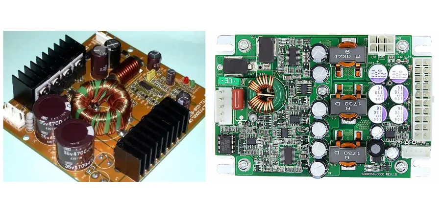
A 48V VRM board guide is essential for engineers designing high-efficiency power delivery networks (PDN) for data centers, automotive EVs, and telecom infrastructure. As power demands for AI accelerators and high-performance computing skyrocket, the industry is shifting from 12V to 48V architecture to reduce $I^2R$ distribution losses. A 48V Voltage Regulator Module (VRM) board steps down this bus voltage to the low voltages (often <1V) required by processors, demanding a PCB design that can handle extreme current densities and thermal stress without failure.
Quick Answer
Designing and manufacturing a 48V VRM board requires strict adherence to thermal and electrical rules to prevent catastrophic failure. Here is the executive summary for immediate application:
- Copper Weight Rule: Standard 1oz copper is rarely sufficient. Use 2oz to 4oz heavy copper on inner layers to handle high current with minimal voltage drop.
- Thermal Pitfall: Neglecting thermal via density under MOSFETs and inductors is the #1 cause of field failure. You must provide a direct thermal path to the chassis or heatsink.
- Layout Criticality: Minimize the loop area of the switching node (SW) to reduce electromagnetic interference (EMI) and voltage spikes.
- Material Selection: Use High-Tg (≥170°C) FR-4 or specialized thermal laminates to withstand continuous operating temperatures above 100°C.
- Verification Method: Perform DC Drop Analysis (IR Drop) simulation before fabrication to ensure voltage drop across the power plane is <1%.
- Manufacturing Check: Verify the etch factor compensation with your CAM engineer; heavy copper requires specific artwork adjustments to maintain trace width integrity.
- Assembly Note: Ensure your stencil design accounts for the volume of solder paste needed for large power components (often requiring 100% aperture opening or step-stencils).
Highlights
- Thermal Management is King: In 48V systems, the PCB itself is a primary heatsink. Layer stackup must be designed for maximum vertical heat transfer.
- Heavy Copper Fabrication: Processing 3oz+ copper requires specialized etching and lamination techniques to prevent voids and delamination.
- Impedance Control: While primarily a power board, the gate drive signals and feedback loops require controlled impedance to prevent false switching.
- Creepage and Clearance: 48V is considered "Safety Extra Low Voltage" (SELV), but tighter component density increases the risk of arcing; strict IPC-2221 clearance rules apply.
- Symmetry Matters: Unbalanced heavy copper stackups will lead to significant board warpage during reflow, causing assembly defects.

48V Vrm Board Guide: Definition and Scope
The transition to 48V architecture is driven by physics: by quadrupling the voltage from 12V to 48V, the current required for the same power level drops by a factor of four, and resistive losses drop by a factor of sixteen. However, this shifts the burden to the VRM board, which must now handle higher input voltages and denser power conversion stages.
A comprehensive 48V VRM board guide covers the entire lifecycle from stackup selection to final assembly. The scope includes selecting materials that resist thermal aging, designing layouts that minimize parasitic inductance, and ensuring the manufacturing process can handle thick copper plating without compromising fine-pitch control signals.
At APTPCB, we often see designs fail not because of the schematic, but because the physical PCB cannot support the thermal or mechanical stresses involved. The decision matrix below outlines how specific fabrication choices impact the final performance of your VRM.
Tech / Decision Lever → Practical Impact
| Decision Lever / Spec | Practical Impact (Yield/Cost/Reliability) |
|---|---|
| Copper Weight (2oz vs. 4oz+) | Heavier copper reduces resistance and heat but increases cost and minimum trace/space limits (making routing harder). |
| Material Tg (150°C vs. 180°C) | High Tg (180°C) is mandatory for VRMs to prevent Z-axis expansion and barrel cracking during thermal cycling. |
| Via Technology (Mechanical vs. Laser) | Laser microvias allow higher density for controller ICs but add cost. Mechanical vias are robust for thermal paths but consume space. |
| Surface Finish (ENIG vs. Immersion Ag) | ENIG offers flat pads for fine-pitch controllers; Immersion Silver is excellent for high-frequency switching but sensitive to handling. |
48V Vrm Board Guide Rules and Specifications
When designing a 48V VRM, "rules of thumb" are often insufficient. You need specific values derived from IPC standards and thermal simulations. Below are the critical specifications we recommend for robust Heavy Copper PCB manufacturing.
| Rule | Recommended Value | Why it matters | How to verify |
|---|---|---|---|
| Min Trace Width (Power) | Calc for $\Delta T < 10^\circ C$ | Prevents traces from acting as fuses. 48V currents can still be high (e.g., 50A+). | IPC-2152 Calculator / Saturn PCB Toolkit. |
| Clearance (48V) | Min 0.25mm (10 mil) | Prevents arcing/leakage, especially with solder mask variations. | DRC (Design Rule Check) in CAD. |
| Thermal Via Pitch | 1.0mm - 1.2mm grid | Optimizes heat spreading without compromising PCB structural integrity. | Visual inspection of Gerber drill files. |
| Solder Mask Dam | Min 4 mil (0.1mm) | Prevents solder bridging on fine-pitch MOSFETs and gate drivers. | CAM Engineering Review (DFM). |
| Dielectric Thickness | Min 3 mil (Prepreg) | Ensures breakdown voltage isolation between layers (Hi-Pot safety). | Stackup report from Fab House. |
| Plating Thickness | Class 3 (avg 25µm) | Ensures via reliability under thermal expansion stress. | Cross-section analysis (Microsection). |
48V Vrm Board Guide Implementation Steps
Moving from schematic to a physical board requires a disciplined process. The high currents involved mean that a layout mistake isn't just a signal integrity issue—it's a fire hazard.
Implementation Process
Step-by-step execution guide
Select a balanced stackup with heavy copper (e.g., 2oz/2oz/2oz/2oz). Choose a High-Tg material (Isola 370HR or equivalent) to handle reflow and operating temps. Consult your fab house early for impedance profiles.
Place input capacitors as close as possible to MOSFETs to minimize loop inductance. Use wide polygons for high-current paths. Keep the switching node compact to reduce radiated EMI.
Stitch the ground planes and power pads with thermal vias. Do not use thermal relief spokes on high-current vias; use solid connections for maximum heat transfer, but adjust soldering profiles accordingly.
Run a DC Drop simulation to verify voltage stability. Submit Gerbers for a DFM review to check heavy copper spacing rules (usually min 8-10 mil space for 3oz copper).
48V Vrm Board Guide Troubleshooting
Even with good design, issues can arise during testing or early production. Here are common failure modes for 48V VRM boards and how to fix them.
1. MOSFET Overheating
- Symptom: Power stage fails or thermal shutdown triggers.
- Root Cause: Insufficient copper area or lack of thermal vias under the exposed pad.
- Fix: Increase the copper pour area on all connected layers. Use High Thermal Conductivity PCB materials or metal-core designs if FR4 is insufficient.
2. Excessive Voltage Ringing (EMI)
- Symptom: High-frequency noise on the output or EMI test failure.
- Root Cause: High parasitic inductance in the input loop or switching node.
- Fix: Move input ceramic capacitors closer to the FETs. Ensure a solid, unbroken ground plane reference directly underneath the high dI/dt loops.
3. Solder Joint Cracking
- Symptom: Intermittent failures after thermal cycling.
- Root Cause: CTE mismatch between the component and the PCB, often exacerbated by low-Tg materials.
- Fix: Upgrade to high-Tg materials (Tg > 170°C) and ensure the plating thickness in vias meets IPC Class 3 requirements to withstand Z-axis expansion.
Supplier Qualification Checklist: How to Vet Your Fab
Not every manufacturer can handle the heavy copper and thermal requirements of a 48V VRM. Use this checklist when selecting a partner like APTPCB.
- Heavy Copper Capability: Can they etch 3oz, 4oz, or 6oz copper with accurate trace definition?
- Thermal Management: Do they offer metal-core (MCPCB) or embedded coin technology if needed?
- Layer Registration: What is their layer-to-layer registration tolerance? (Critical for high-layer-count power boards).
- Cross-Section Analysis: Do they perform micro-sections on every batch to verify plating thickness and wall quality?
- Hi-Pot Testing: Can they perform high-voltage testing to ensure dielectric breakdown compliance?
- Impedance Control: Do they provide TDR reports for the gate drive and communication lines?
Glossary
- VRM (Voltage Regulator Module): A buck converter that steps down voltage (e.g., 48V to 1V) for processors.
- PDN (Power Delivery Network): The complete path of power from the source to the load, including PCB traces, planes, and capacitors.
- Tg (Glass Transition Temperature): The temperature at which the PCB substrate transitions from a rigid to a soft state. High Tg is crucial for power boards.
- DCR (DC Resistance): The resistance of a component (like an inductor) or trace at 0Hz, causing power loss ($I^2R$).
- Creepage: The shortest distance between two conductive parts along the surface of the insulation.
6 Essential Rules for 48V Vrm Board Guide (Cheat Sheet)
| Rule / Guideline | Why It Matters (Physics/Cost) | Target Value / Action |
|---|---|---|
| Minimize Input Loop Area | High dI/dt creates voltage spikes ($V = L \cdot di/dt$). Large loops = blown FETs. | < 2mm distance (Caps to FETs) |
| Maximize Copper Weight | Reduces resistive heating and voltage drop. | 2oz - 4oz (Inner layers) |
| Continuous Ground Plane | Provides return path and shielding. Cuts in plane increase inductance. | No splits under power stage |
| Thermal Via Density | Moves heat from top layer components to inner/bottom planes. | 1.0mm pitch (Under pads) |
| Gate Drive Isolation | Prevents power noise from triggering false switching. | 20 mil spacing from SW node |
| Symmetrical Stackup | Prevents warping (potato chipping) during reflow with heavy copper. | Mirror copper weights |
FAQ
Q: Why is 48V preferred over 12V for modern data centers?
A: 48V reduces current by 4x compared to 12V for the same power. Since power loss is proportional to the square of the current ($I^2R$), this reduces distribution losses by 16x, allowing for thinner busbars and higher efficiency.
Q: Can I use standard FR-4 for a 48V VRM board?
A: For low-power applications, yes. However, for high-density VRMs, standard FR-4 (Tg 130-140°C) may degrade or delaminate. We strongly recommend High-Tg FR-4 (Tg ≥ 170°C) or specialized thermal materials.
Q: What is the minimum trace width for 48V power traces?
A: There is no single "minimum." It depends on the current and allowed temperature rise. Use IPC-2152 charts. For example, to carry 20A with a 10°C rise on 2oz copper, you might need a trace width of roughly 300-400 mils (7-10mm), or use planes.
Q: Do I need blind or buried vias for VRM boards?
A: Not always, but they help in high-density designs. Blind vias allow you to route gate drive signals on outer layers without perforating the inner power planes, preserving the current-carrying capacity of the internal layers.
Q: How do I specify heavy copper in my fabrication notes?
A: Clearly state the finished copper weight for each layer in the stackup table (e.g., "Layer 2: 3oz Cu"). Also, specify "UL approved heavy copper process" to ensure the fab uses the correct etching compensation.
Q: What surface finish is best for 48V VRM boards?
A: ENIG (Electroless Nickel Immersion Gold) is excellent for planarity and fine-pitch components. Immersion Silver is also good for conductivity but requires careful handling. HASL is generally avoided due to uneven surfaces on fine-pitch pads.
Request a Quote / DFM Review for 48V Vrm Board Guide
Ready to manufacture your high-power VRM design? The engineering team at APTPCB specializes in heavy copper and thermal management solutions.
Send us the following for a comprehensive DFM review:
- Gerber Files (RS-274X format preferred).
- Stackup Diagram specifying copper weights (e.g., 2oz, 3oz, 4oz).
- Drill Files (NC Drill).
- Fabrication Drawing with notes on Tg requirements and solder mask color.
- Netlist (IPC-356) for electrical verification.
Conclusion
Designing a successful 48V VRM board is a balancing act between electrical efficiency, thermal dissipation, and manufacturability. By adhering to heavy copper rules, optimizing your thermal via strategy, and selecting the right materials, you can build power modules that are both efficient and reliable. Don't let the layout be the bottleneck in your power delivery network.
Signed, The Engineering Team at APTPCB