Contents
- Highlights
- 5G Balun PCB: Definition and Scope
- 5G Balun PCB Rules and Specifications
- 5G Balun PCB Implementation Steps
- 5G Balun PCB Troubleshooting
- Supplier Qualification Checklist: How to Vet Your Fab
- Glossary
- 6 Essential Rules for 5G Balun PCB (Cheat Sheet)
- FAQ
- Request a Quote / DFM Review for 5G Balun PCB
- Conclusion
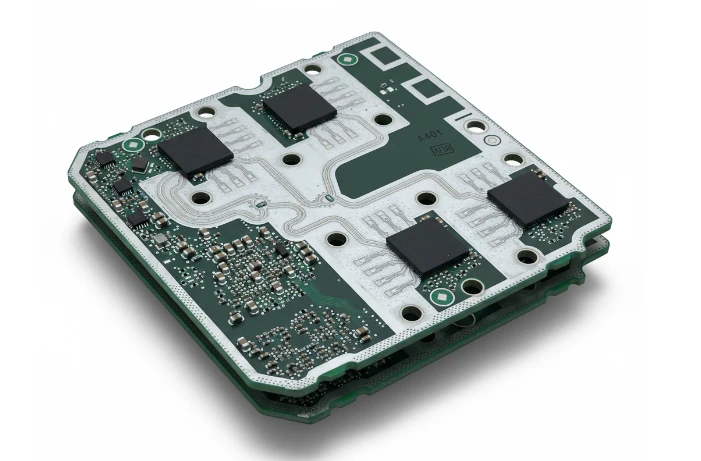
In the architecture of 5G networks—specifically within Active Antenna Units (AAU) and massive MIMO arrays—the 5G Balun PCB plays a silent but critical role. A Balun (Balanced-to-Unbalanced) is a transformer that converts differential signals (balanced) to single-ended signals (unbalanced) or matches differing impedances. In the context of 5G mmWave and Sub-6GHz frequencies, the "Balun PCB" refers to the specific layout, material stackup, and fabrication techniques required to integrate these components (often printed directly onto the PCB or embedded) without catastrophic signal loss or phase distortion.
As a Senior CAM Engineer at APTPCB, I often see designs fail not because the schematic was wrong, but because the physical realization of the Balun on the PCB ignored the physics of high-frequency manufacturing. At frequencies exceeding 28GHz, a 1-mil variation in trace width or a slight surface roughness in the copper can destroy the phase balance required for beamforming.
Quick Answer
If you are designing or procuring a 5G Balun PCB, here is the immediate technical summary:
- Impedance Control: You are typically matching 50Ω single-ended to 100Ω differential. Tolerance must be held to ±5% or tighter (standard ±10% is insufficient for 5G efficiency).
- Material Selection: Standard FR4 is unacceptable for the RF layer. You must use high-frequency laminates (e.g., Rogers RO4350B, RO3003, or Panasonic Megtron 7) with a Dissipation Factor (Df) < 0.003.
- Critical Pitfall: Passive Intermodulation (PIM) caused by the wrong surface finish. Avoid HASL. Use Immersion Silver or ENIG (though watch for nickel resonance at very high frequencies).
- Verification: Do not rely solely on DC continuity. You must require TDR (Time Domain Reflectometry) testing for impedance and, ideally, VNA testing for S-parameters (Insertion Loss/Return Loss) on test coupons.
- Layout Rule: Symmetry is absolute. Any length mismatch between the differential legs of the Balun converts common-mode noise into differential noise, ruining the Signal-to-Noise Ratio (SNR).
Highlights
- Phase Balance is King: For 5G beamforming, phase errors >5° can degrade antenna gain significantly. PCB etching precision is the primary driver of phase accuracy.
- Hybrid Stackups: To manage costs, we often build 5G Balun PCBs using a hybrid structure—expensive PTFE/Ceramic cores for the RF Balun layer and standard FR4 for digital control/power layers.
- Copper Roughness: At mmWave frequencies, the "skin depth" of the signal is shallow. Standard copper foil is too rough and acts like a resistor. Specify HVLP (Hyper Very Low Profile) copper.
- Thermal Management: Baluns in 5G Power Amplifiers (PAs) handle significant RF power. Thermal vias and metal-core backings are often required to prevent frequency drift due to heat.
5G Balun PCB: Definition and Scope
A 5G Balun PCB is rarely a standalone board; it is usually a sub-section of a larger Transceiver (TRX) board or an Antenna Integration Board (AIB). Its primary function is to interface the Power Amplifier (PA) or Low Noise Amplifier (LNA)—which often operate in push-pull (differential) modes—with the antenna element (usually single-ended).
In 5G applications, we see two main types of Balun implementations on PCBs:
- Discrete Component Balun: A physical ceramic component soldered onto the PCB. The PCB challenge here is minimizing parasitic capacitance at the landing pads and ensuring the transmission lines leading to it are perfectly matched.
- Printed Balun: The transformer structure is etched directly into the copper (e.g., Marchand Balun, Rat-Race Coupler). This is common in mmWave because discrete components become lossy and expensive. Here, the PCB manufacturing tolerance becomes the component specification.
The manufacturing complexity arises because 5G signals are extremely sensitive to the dielectric constant (Dk) of the material. If the resin content varies across the board (resin starvation), the Dk changes, shifting the center frequency of the Balun.
Tech / Decision Lever → Practical Impact
| Decision Lever / Spec | Practical Impact (Yield/Cost/Reliability) |
|---|---|
| Substrate Material (PTFE vs. FR4) | PTFE (e.g., Rogers) ensures low signal loss but increases cost by 3-5x and requires specialized plasma etching for via reliability. |
| Copper Foil Profile (Standard vs. HVLP) | HVLP reduces insertion loss by 15-20% at 28GHz. Standard copper creates "resistive" losses due to skin effect. |
| Etching Tolerance (±10% vs. ±5%) | ±5% is mandatory for Printed Baluns. Looser tolerance leads to phase imbalance, reducing 5G data throughput and range. |
| Surface Finish (ENIG vs. Immersion Ag) | Immersion Silver is preferred for 5G. The Nickel layer in ENIG can cause magnetic losses and PIM issues at high frequencies. |
5G Balun PCB Rules and Specifications
When moving from prototype to mass production, vague specifications are the enemy. Below are the specific rules we enforce at APTPCB for High Frequency PCB fabrication involving Baluns.
| Rule | Recommended Value | Why it matters | How to verify |
|---|---|---|---|
| Impedance Tolerance | ±5% (or ±2Ω) | Baluns rely on precise impedance transformation. Mismatches cause signal reflection (VSWR). | TDR Coupon Test (IPC-TM-650 2.5.5.7) |
| Dielectric Constant (Dk) Stability | ±0.05 across panel | Variations shift the Balun's operating frequency band. | Verify laminate datasheet & ask for Dk uniformity test data. |
| Copper Etch Factor | ≥ 3.0 | Trapezoidal traces change the effective impedance compared to rectangular assumptions. | Cross-section analysis (Microsection). |
| Registration Accuracy | ±3 mil (0.075mm) | Misalignment between the signal layer and the ground reference plane alters impedance. | X-Ray Inspection of layer alignment. |
| Solder Mask Opening | Keep-out over RF lines | Solder mask has a high Df and adds loss. Printed Baluns should be bare copper (plated) or covered only by OSP/Silver. | Visual Inspection / Gerber Review. |
5G Balun PCB Implementation Steps
Successfully manufacturing a 5G Balun PCB requires a synchronized effort between the design engineer and the CAM engineer. Here is the process flow we utilize.
Implementation Process
Step-by-step execution guide
Select low-loss laminates (Rogers/Taconic). Decide on a hybrid stackup (RF core + FR4 prepreg) to balance performance and cost. Consult our Rogers PCB guide for specific grades.
CAM engineers adjust trace widths to account for etch-back. For 5G Baluns, we apply strict compensation to ensure the final top width matches the simulation design, not just the phototool.
Utilize Laser Direct Imaging (LDI) for trace definition. Plating thickness must be uniform; excess plating on the edges of a printed Balun changes its coupling coefficient.
Perform TDR testing on impedance coupons. For critical 5G applications, we may perform S-parameter testing (Insertion Loss) to verify the material Df hasn't drifted during lamination.
5G Balun PCB Troubleshooting
Even with good design, manufacturing variables can cause failures. Here are common issues we diagnose in the lab:
1. High Insertion Loss
If the signal is attenuating more than simulated, check the Surface Roughness. If the copper foil on the laminate is standard profile (Rz > 5µm), the skin effect at 28GHz will cause massive losses.
- Fix: Specify VLP (Very Low Profile) or HVLP copper in the fabrication notes. Also, verify that the solder mask was removed from the RF traces.
2. Phase Imbalance
If the differential signals are not 180° out of phase, the Balun fails to cancel common-mode noise. This is often caused by Etching Non-Uniformity. If the spacing between coupled lines varies along the length, the odd-mode impedance changes.
- Fix: Use LDI (Laser Direct Imaging) rather than traditional film exposure. Ensure the manufacturer uses "nested" coupons to check etching consistency across the panel.
3. Passive Intermodulation (Pim)
Unexpected noise floors or signal distortion can arise from the Surface Finish.
- Fix: Avoid ENIG if the nickel layer is not strictly controlled, as nickel is ferromagnetic. Immersion Silver or OSP are safer choices for pure RF performance.
Supplier Qualification Checklist: How to Vet Your Fab
Before awarding a contract for 5G Balun PCBs, ask your supplier these specific questions to gauge their capability.
- Do you have in-house plasma cleaning capabilities? (Essential for activating PTFE surfaces before plating vias).
- What is your minimum trace/space tolerance for RF layers? (Should be ±0.5 mil or better for mmWave).
- Do you use Laser Direct Imaging (LDI) for all RF layers? (Film exposure is not accurate enough for 5G phase matching).
- Can you provide TDR reports for differential impedance at 100Ω?
- Do you have experience with hybrid stackups (e.g., Rogers + FR4)? (Ask for photos of cross-sections to check for delamination risks).
- How do you measure copper roughness? (They should know what Rz and Rq values are).
- Do you offer X-Ray inspection for layer-to-layer registration?
Glossary
Balun: A device that converts between Balanced (differential) and Unbalanced (single-ended) signals. Essential for connecting antennas (often single-ended) to differential amplifiers.
Skin Effect: The tendency of high-frequency alternating current (AC) to flow only near the surface of the conductor. This makes the surface roughness of the copper critical for 5G PCBs.
PIM (Passive Intermodulation): Signal distortion caused by non-linearities in passive components, often due to poor solder joints, ferromagnetic materials (like Nickel), or rough copper surfaces.
Hybrid Stackup: A PCB construction method that combines different materials (e.g., expensive high-frequency laminates for RF layers and cheaper FR4 for digital layers) to optimize cost and performance.
LDI (Laser Direct Imaging): A manufacturing process where the circuit pattern is written directly onto the PCB resist using a laser, offering much higher precision than traditional film-based photolithography.
6 Essential Rules for 5G Balun PCB (Cheat Sheet)
| Rule / Guideline | Why It Matters (Physics/Cost) | Target Value / Action |
|---|---|---|
| Symmetry is Non-Negotiable | Asymmetry converts common-mode noise to differential noise, ruining SNR. | < 5 mil length mismatch |
| Ground Via Fencing | Prevents signal leakage and crosstalk between the Balun and other circuits. | λ/20 spacing max |
| Remove Solder Mask | Solder mask has high Df (~0.02) compared to air/Rogers, causing loss. | Solder Mask Opening over RF traces |
| Use HVLP Copper | Rough copper increases effective resistance at mmWave frequencies. | Rz < 2µm |
| Continuous Reference Plane | Return path current must flow directly under the signal. Gaps cause inductance spikes. | Solid Copper (No splits) |
| Thermal Vias for PA | Baluns near PAs get hot; heat changes the Dk of the substrate, shifting frequency. | Filled/Capped Vias under pads |
FAQ
Q: Can I use standard FR4 for a 5G Balun PCB to save money?
A: Generally, no. For Sub-6GHz (e.g., 3.5GHz), you might get away with high-performance FR4 (like Isola FR408HR), but for mmWave (28GHz+), standard FR4 is too lossy (high Df) and inconsistent. The signal will be absorbed by the board. We recommend a hybrid stackup using Rogers PCB materials for the RF layer and FR4 for the rest.
Q: Why is Immersion Silver preferred over ENIG for 5G PCBs?
A: ENIG (Electroless Nickel Immersion Gold) contains a layer of Nickel. Nickel is ferromagnetic, which can cause magnetic losses and generate Passive Intermodulation (PIM) at high frequencies. Immersion Silver provides excellent conductivity without the magnetic downsides, though it requires careful handling to prevent tarnishing.
Q: How do I calculate the trace width for a printed Balun?
A: You cannot use simple online calculators. Printed Baluns (like tapered lines) require electromagnetic simulation software (like ADS or HFSS). However, for the transmission lines leading to the Balun, you can use our Impedance Calculator as a starting point, but always validate with the fab's specific stackup data.
Q: What is the biggest manufacturing risk for 5G Baluns?
A: Etching variation. If the gap between coupled lines in a Balun varies by even 0.5 mil, the coupling coefficient changes, ruining the phase balance. This is why we use LDI (Laser Direct Imaging) for these critical layers.
Q: Do I need back-drilling for 5G Balun PCBs?
A: If your signal transitions through vias (e.g., from Top to Layer 3), the unused portion of the via (the stub) acts as an antenna that causes resonance and signal reflection. For 5G data rates, back-drilling is almost always required to remove these stubs and preserve signal integrity.
Q: How do you handle heat dissipation for Baluns connected to Power Amplifiers?
A: We often use Metal Core PCB technology or embedded copper coins. Alternatively, dense arrays of thermal vias plugged with conductive epoxy are placed directly under the component thermal pads to shunt heat to a bottom-side heatsink.
Request a Quote / DFM Review for 5G Balun PCB
Ready to move your 5G design from simulation to reality? To get an accurate quote and a comprehensive DFM (Design for Manufacturing) review, please prepare the following:
- Gerber Files (RS-274X): Ensure RF layers are clearly marked.
- Stackup Diagram: Specify the exact laminate (e.g., Rogers RO4350B 10mil) and copper weight.
- Impedance Requirements: List target impedances (e.g., 50Ω SE, 100Ω Diff) and the specific layers/traces they apply to.
- Drill File: Identify any back-drill requirements.
- Surface Finish Preference: (e.g., Immersion Silver, OSP, or ENIG).
Conclusion
Designing a 5G Balun PCB is an exercise in balancing electromagnetic theory with manufacturing reality. The transition from differential to single-ended signals at mmWave frequencies tolerates zero errors in material selection or etching precision. By adhering to strict symmetry, utilizing hybrid stackups, and partnering with a manufacturer capable of LDI and VNA testing, you can ensure your 5G front-end performs as simulated.
At APTPCB, we specialize in these high-frequency challenges. Whether you need a prototype on Rogers material or a mass-production hybrid build, we have the engineering depth to support you.
Signed, The Engineering Team at APTPCB