Contents
- Highlights
- 5G Base Station PCB: Definition and Scope
- 5G Base Station PCB Rules and Specifications
- 5G Base Station PCB Implementation Steps
- 5G Base Station PCB Troubleshooting
- Supplier Qualification Checklist: How to Vet Your Fab
- Glossary
- 6 Essential Rules for 5G Base Station PCB (Cheat Sheet)
- FAQ
- Request a Quote / DFM Review for 5G Base Station PCB
- Conclusion
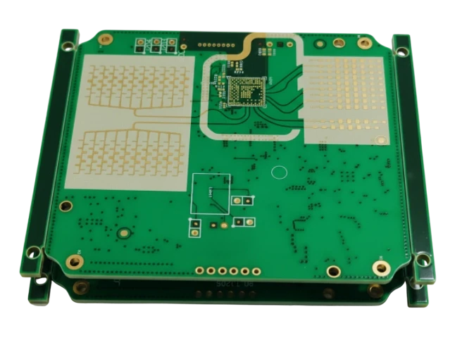
As a Senior CAM Engineer at APTPCB, I review hundreds of Gerber files for telecommunications infrastructure every month. A 5G Base Station PCB is not a standard circuit board; it is a high-performance interconnect system that must handle massive data throughput (Massive MIMO), millimeter-wave frequencies, and intense thermal loads simultaneously. These boards typically function within the Active Antenna Unit (AAU) or the Baseband Unit (BBU), requiring a complex mix of high-frequency laminates and high-speed digital logic layers.
If you treat a 5G base station design like a standard FR4 board, it will fail—either through signal loss, thermal runaway, or Passive Intermodulation (PIM). This guide covers the specific manufacturing rules, material choices, and verification steps we use on the factory floor to ensure these critical components perform in the field.
Quick Answer
For engineers and procurement teams in a rush, here are the critical parameters for successful 5G Base Station PCB fabrication:
- Material Strategy: Use Hybrid Stackups. Combine high-frequency materials (like Rogers or Taconic) for RF layers with high-Tg FR4 for digital/power layers to balance cost and performance.
- Copper Profile: Specify HVLP (High Very Low Profile) copper foil. Standard copper roughness creates a "skin effect" that destroys signal integrity at 5G frequencies (28GHz+).
- Thermal Management: 5G Power Amplifiers (PAs) generate immense heat. Design with embedded copper coins or dense thermal via arrays plugged with conductive resin.
- PIM Control: For antenna layers, avoid solder mask over RF traces if possible. Use Immersion Silver or Immersion Tin finishes; ENIG can introduce non-linearities that degrade PIM performance.
- Layer Registration: High layer counts (12-24 layers) in BBUs require strict registration tolerance (±3 mil) to ensure backdrilled stubs hit the target without damaging internal traces.
- Verification: Always request PIM Testing (Passive Intermodulation) and TDR (Time Domain Reflectometry) impedance reports for every production batch.
- Drilling: Backdrilling is mandatory for high-speed links (>10 Gbps) to remove via stubs that act as antennas and cause signal reflection.
Highlights
- Hybrid Lamination Mastery: How to mix CTE-mismatched materials without causing delamination during reflow.
- Thermal Dissipation: Techniques for managing the high heat flux of 5G AAUs using metal cores and copper coins.
- Signal Integrity: The impact of copper roughness and dielectric loss (Df) on mmWave performance.
- Manufacturing Tolerances: Why standard IPC Class 2 tolerances are often insufficient for 5G interconnects.
5G Base Station PCB: Definition and Scope
The 5G infrastructure ecosystem is divided primarily into the AAU (Active Antenna Unit), which integrates the antenna and RF frontend, and the BBU (Baseband Unit) / CU (Centralized Unit) / DU (Distributed Unit), which handles processing.
AAU PCBs are the most challenging to manufacture. They require low-loss materials to transmit RF signals efficiently and high thermal conductivity to dissipate heat from power amplifiers. These are often large-format boards utilizing High Frequency PCB technologies.
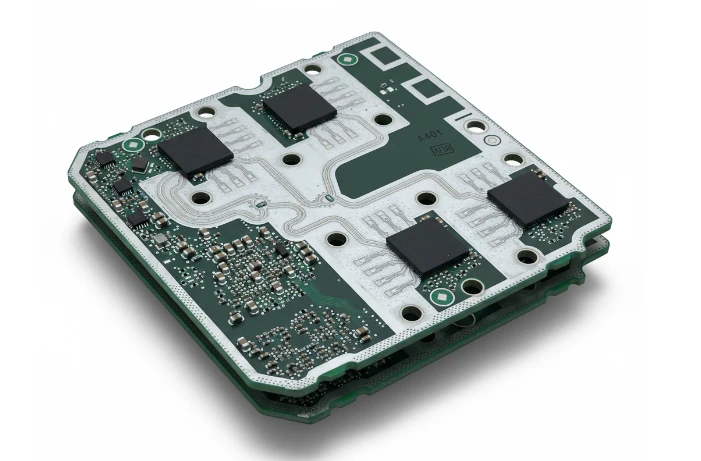
BBU PCBs resemble high-end server boards. They are characterized by high layer counts (20+ layers), high-speed digital lines (PCIe Gen 4/5, CPRI), and require Backplane PCB manufacturing techniques.
The decision matrix below outlines how specific design levers impact the final production yield and performance of these boards.
Tech / Decision Lever → Practical Impact
| Decision Lever / Spec | Practical Impact (Yield/Cost/Reliability) |
|---|---|
| Hybrid Stackup (Rogers + FR4) | Reduces material cost by 30-50% vs. pure PTFE. Risk: Warpage due to CTE mismatch if stackup is not symmetric. |
| Embedded Copper Coin | Provides localized cooling for PAs (Power Amplifiers). Cost: Increases PCB cost by 20-30% but eliminates bulky external heatsinks. |
| Backdrilling (Controlled Depth) | Essential for signal integrity >10Gbps. Yield: Requires precise Z-axis control; poor execution cuts internal connections. |
| Immersion Silver Finish | Best for PIM performance and flatness. Storage: Sensitive to tarnishing; requires strict handling and vacuum packaging. |
5G Base Station PCB Rules and Specifications
When designing or ordering these boards, vague specifications lead to production holds. We recommend the following specific parameters based on our experience manufacturing Antenna PCBs and high-speed digital boards.
| Rule | Recommended Value | Why it matters | How to verify |
|---|---|---|---|
| Dielectric Constant (Dk) | 3.0 - 3.5 (RF Layers) | Low Dk reduces signal delay and capacitance. Stability over frequency is crucial for 5G. | Review material datasheet (e.g., Rogers 4350B, Megtron 6). |
| Dissipation Factor (Df) | < 0.003 @ 10GHz | Minimizes signal loss (attenuation) over long trace lengths in AAUs. | Network Analyzer test on test coupons. |
| Copper Roughness | Rz < 2.0 µm (HVLP) | At mmWave, current flows in the "skin" of the copper. Roughness increases resistance and loss. | Cross-section analysis (Microsection). |
| Impedance Tolerance | ±5% or ±7% | 5G systems are highly sensitive to impedance mismatches causing reflections. | TDR (Time Domain Reflectometry) testing on coupons. |
| Thermal Conductivity | > 1.0 W/m-K (Dielectric) | High power density in 5G chips requires dielectric materials that help move heat. | Thermal simulation and material certification. |
| Via Plugging | VIPPO (Via-in-Pad Plated Over) | Required for BGA components with 0.4mm-0.5mm pitch to prevent solder wicking. | Visual inspection and X-Ray. |
5G Base Station PCB Implementation Steps
Implementing a successful 5G PCB build requires a synchronized effort between the design team and the CAM engineers. Here is the step-by-step execution guide we follow at APTPCB.
Implementation Process
Step-by-step execution guide
Define the hybrid structure. Place high-frequency laminates (e.g., Rogers RO4350B) on outer layers for RF signals and high-Tg FR4 (e.g., IT-180) in the core for mechanical stability and power distribution. Ensure resin content is sufficient to fill voids in high-copper layers.
Execute mechanical drilling for through-holes and laser drilling for micro-vias. Perform Backdrilling on high-speed signal vias to remove unused stubs. This step is critical for reducing signal reflection in 25Gbps+ links.
Etch traces with strict width compensation to meet impedance goals. Apply surface finish—typically Immersion Silver or OSP for RF sections to minimize PIM, and ENIG for digital sections if selective finishing is possible (or use Immersion Silver globally).
Conduct 100% AOI (Automated Optical Inspection). Perform TDR impedance testing on coupons. For antenna boards, perform PIM testing to ensure the passive intermodulation is within spec (typically < -160 dBc).
5G Base Station PCB Troubleshooting
Even with perfect design, manufacturing issues can arise. Here are common failure modes we see in 5G PCBs and how to fix them.
1. Delamination in Hybrid Stackups
Problem: The Rogers material and FR4 material expand at different rates during reflow soldering (CTE mismatch), causing layers to separate. Fix: Use "Low-Flow" prepregs specifically designed for bonding dissimilar materials. Ensure the stackup is symmetrical. Bake the boards before assembly to remove moisture.
2. High Pim (Passive Intermodulation)
Problem: The antenna generates interference signals, degrading network performance. Fix: Check the copper etching quality; under-etching leaves jagged edges that cause PIM. Ensure no solder mask covers the high-frequency RF lines. Switch from ENIG to Immersion Silver or Tin.
3. Signal Attenuation Higher Than Simulated
Problem: The real-world signal loss is worse than the simulation predicted. Fix: The simulation likely assumed smooth copper. Verify that the fabricator used HVLP (High Very Low Profile) or VLP copper foil. Standard ED copper is too rough for 5G mmWave frequencies.
Supplier Qualification Checklist: How to Vet Your Fab
Not every PCB factory can handle the complexity of Multilayer PCB structures required for 5G. Use this checklist to vet your supplier:
- Hybrid Lamination Experience: Can they show examples of successful Rogers + FR4 hybrid builds?
- Backdrilling Capability: What is their backdrill depth tolerance? (Should be ±0.1mm or better).
- PIM Testing: Do they have in-house PIM testing equipment, or do they outsource it?
- Copper Profile Control: Do they stock HVLP copper foils and understand the impact on skin effect?
- Registration Accuracy: Can they achieve layer-to-layer registration of < 3 mil for high-layer count boards?
- Thermal Solutions: Do they have experience embedding copper coins or manufacturing metal-core hybrid boards?
Glossary
Massive MIMO (Multiple Input Multiple Output): A technology used in 5G AAUs where large arrays of antennas transmit and receive data simultaneously to increase capacity. PIM (Passive Intermodulation): Signal distortion caused by non-linearities in passive components (like PCB traces, connectors, or surface finishes), critical in 5G networks. Hybrid Stackup: A PCB layer buildup that uses expensive high-frequency materials only on critical signal layers and cheaper FR4 on other layers to save cost. Skin Effect: The tendency of high-frequency alternating current to flow near the surface of the conductor. At 5G frequencies, this makes copper surface roughness a major factor in signal loss. Backdrilling: The process of drilling out the unused portion of a plated through-hole (via stub) to reduce signal reflection in high-speed circuits.
6 Essential Rules for 5G Base Station PCB (Cheat Sheet)
| Rule / Guideline | Why It Matters (Physics/Cost) | Target Value / Action |
|---|---|---|
| Use Hybrid Materials | Optimizes cost while maintaining RF performance. | Rogers/Taconic + High-Tg FR4 |
| Specify HVLP Copper | Rough copper increases insertion loss at mmWave frequencies. | Roughness (Rz) < 2.0µm |
| Implement Backdrilling | Via stubs act as antennas, causing signal reflection >10Gbps. | Stub length < 10 mil |
| Thermal Management | 5G PAs generate high heat; dielectric alone cannot dissipate it. | Embedded Coins / Thermal Vias |
| PIM-Friendly Finish | Nickel in ENIG is ferromagnetic and causes PIM issues. | Immersion Silver / Tin |
| Impedance Control | Critical for signal integrity in RF and high-speed digital lines. | Tolerance ±5% |
FAQ
Q: Why is Immersion Silver preferred over ENIG for 5G PCBs?
A: ENIG (Electroless Nickel Immersion Gold) contains nickel, which is ferromagnetic. In high-power RF applications, this magnetic property can generate non-linear Passive Intermodulation (PIM) distortion. Immersion Silver is non-magnetic and offers excellent surface flatness and conductivity, making it ideal for 5G antenna layers.
Q: Can I use standard FR4 for 5G Base Station PCBs?
A: Generally, no. Standard FR4 has a high Dissipation Factor (Df ~0.02) which causes excessive signal loss at 5G frequencies (sub-6GHz and mmWave). However, high-performance FR4 (like Megtron 6 or IT-968) can be used for digital layers or in hybrid stackups, but the RF signal path usually requires PTFE or ceramic-filled hydrocarbon materials.
Q: What is the biggest manufacturing challenge with Hybrid Stackups?
A: The primary challenge is the difference in Coefficient of Thermal Expansion (CTE) and scaling factors between the RF material (e.g., Rogers) and the FR4. If not managed correctly during lamination, this leads to warping, delamination, or layer misregistration.
Q: How do you manage heat in 5G AAU PCBs?
A: We use several techniques: selecting substrates with high thermal conductivity (TC), using heavy copper layers (2oz+), implementing dense arrays of thermal vias (VIPPO), and for extreme heat, embedding solid copper coins directly under the Power Amplifier components.
Q: What is the typical layer count for a 5G BBU PCB?
A: 5G Baseband Units (BBUs) are complex computing nodes. Their PCBs typically range from 14 to 24 layers, often utilizing HDI (High Density Interconnect) technology with multiple lamination cycles to route the high density of connections.
Q: Do I need backdrilling for all 5G PCBs?
A: Not necessarily for the antenna board if it is a simple double-sided design, but for the BBU and high-speed digital sections, backdrilling is almost always required to remove via stubs that would otherwise degrade signal integrity at data rates above 10 Gbps.
Request a Quote / DFM Review for 5G Base Station PCB
Ready to move your 5G design to production? At APTPCB, we specialize in high-frequency and hybrid stackup manufacturing. To get an accurate quote and a comprehensive DFM (Design for Manufacturing) review, please prepare the following:
- Gerber Files: RS-274X or ODB++ format.
- Fabrication Drawing: Clearly specify material types (e.g., "Rogers 4350B + IT-180"), copper weights, and surface finish.
- Stackup Diagram: Detail the layer order and dielectric thicknesses.
- Drill Chart: Identify plated vs. non-plated holes and any backdrilling requirements.
- Impedance Requirements: List target impedance values and reference layers.
- Special Requirements: Note any embedded coins, PIM testing needs, or specific IPC class requirements (Class 2 or 3).
Conclusion
Manufacturing 5G Base Station PCBs requires a departure from standard PCB fabrication rules. It demands a deep understanding of material science, strict control over copper roughness and etching tolerances, and advanced thermal management strategies. By choosing the right hybrid materials, specifying HVLP copper, and partnering with a manufacturer experienced in PIM control and backdrilling, you can ensure your base station hardware delivers the speed and reliability the 5G network promises.
Signed, The Engineering Team at APTPCB