Contents
- Highlights
- 5G Du PCB: Definition and Scope
- 5G Du PCB Rules and Specifications
- 5G Du PCB Implementation Steps
- 5G Du PCB Troubleshooting
- Supplier Qualification Checklist: How to Vet Your Fab
- Glossary
- 6 Essential Rules for 5G Du PCB (Cheat Sheet)
- FAQ
- Request a Quote / DFM Review for 5G Du PCB
- Conclusion
In the architecture of 5G networks, the 5G DU PCB (Distributed Unit) acts as the computational engine that bridges the gap between the centralized core and the radio edge. Unlike the AAU (Active Antenna Unit) which handles RF transmission, the DU is responsible for real-time baseband processing and high-speed data transport via eCPRI interfaces. For PCB designers and CAM engineers, a 5G DU board represents a convergence of high-speed digital design, thermal management, and strict signal integrity requirements.
These boards function essentially as high-performance servers deployed in telecom environments. They must handle massive data throughput (often 25 Gbps to 56 Gbps per lane) while surviving outdoor cabinet conditions. This guide breaks down the manufacturing realities of building reliable 5G DU PCBs.
Quick Answer
To manufacture a functional 5G DU PCB, you must prioritize signal integrity over standard FR4 cost savings.
- Critical Rule: Use Ultra-Low Loss materials (Df < 0.004 @ 10GHz) such as Panasonic Megtron 6/7 or Isola Tachyon. Standard FR4 is insufficient for DU signal speeds.
- Common Pitfall: Neglecting Backdrilling. At 25Gbps+, via stubs act as antennas, causing severe signal reflection and data loss.
- Verification: Mandatory TDR (Time Domain Reflectometry) testing for impedance control (±5% or ±8%) and VNA testing for insertion loss.
Highlights
- Material Selection: Requires high-speed laminates with low dielectric constant (Dk) and dissipation factor (Df) to minimize signal attenuation.
- Backdrilling: Essential for removing unused via stubs on high-speed differential pairs (e.g., PCIe Gen 4/5, eCPRI).
- Layer Count: Typically ranges from 14 to 26 layers, often requiring multiple lamination cycles.
- Copper Profile: Usage of HVLP (Hyper Very Low Profile) copper foil to reduce skin effect losses at high frequencies.
- Thermal Design: Heavy reliance on thermal vias and potentially embedded copper coins to cool high-power FPGAs and ASICs.
5G Du PCB: Definition and Scope
The 5G RAN (Radio Access Network) is split into three parts: the CU (Centralized Unit), the DU (Distributed Unit), and the RU (Radio Unit). The 5G DU PCB is the hardware platform for the Distributed Unit. It processes Layer 1 (Physical) and Layer 2 (MAC/RLC) protocols in real-time.
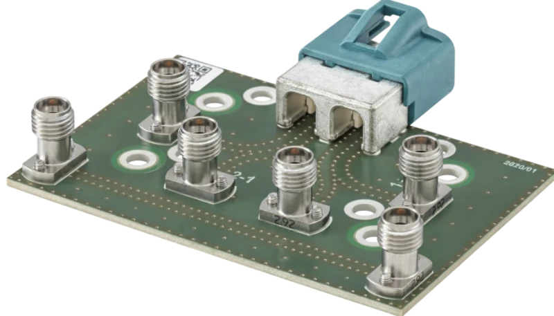
Physically, a DU PCB resembles a complex High-Speed PCB or a telecom backplane. It is densely populated with BGA components (FPGAs, DSPs), optical cages (SFP28/QSFP28), and high-speed connectors. The manufacturing challenge lies in maintaining signal integrity across long trace lengths while managing the heat generated by intensive processing.
Unlike the AAU, which is RF-analog heavy, the DU is digital-heavy. However, the "digital" signals are so fast that they exhibit analog behaviors, requiring RF-like precision in manufacturing.
Tech / Decision Lever → Practical Impact
| Decision Lever / Spec | Practical Impact (Yield/Cost/Reliability) |
|---|---|
| Material: Megtron 7 vs. FR4 | Megtron 7 reduces insertion loss by >50% at 25GHz. Cost Impact: 3-4x higher raw material cost, but essential for functionality. |
| Backdrilling (Stub Removal) | Reduces deterministic jitter. Yield Impact: Adds a drill process; requires precise depth control (±0.05mm) to avoid damaging internal layers. |
| HVLP Copper Foil | Smoother copper reduces "skin effect" losses. Reliability Impact: Improves signal eye diagram opening; requires careful bonding treatment to prevent delamination. |
| Impedance Tolerance ±5% | Tighter control than standard ±10%. Yield Impact: Requires strict etching compensation and consistent dielectric thickness pressing. |
5G Du PCB Rules and Specifications
Designing and fabricating a DU PCB requires adherence to strict specifications to ensure the board can handle the bandwidth requirements of 5G.
| Rule / Spec | Recommended Value | Why it matters | How to verify |
|---|---|---|---|
| Material Df (Dissipation Factor) | < 0.005 @ 10GHz | High Df causes signal energy to be absorbed by the dielectric, killing range and data integrity. | Review IPC-4101 sheet; verify laminate brand (e.g., Megtron PCB). |
| Backdrill Stub Length | < 10 mil (0.25mm) | Long stubs create reflections (resonance) that destroy high-speed signals. | Cross-section analysis (microsection) after drilling. |
| Impedance Control | 85Ω / 100Ω ±8% | Mismatched impedance causes signal reflection (return loss). | TDR (Time Domain Reflectometry) coupons on production panels. |
| Copper Roughness | Rz < 2.0µm (HVLP) | Rough copper increases resistance at high frequencies due to skin effect. | SEM (Scanning Electron Microscope) or supplier certs. |
| Via Aspect Ratio | 10:1 to 12:1 | Ensures reliable plating in thick boards (2.0mm - 3.0mm). | Cross-section to measure plating thickness in hole center. |
| Glass Weave Style | Spread Glass (1067/1078) | Prevents "Fiber Weave Effect" (skew) where differential pairs travel over gaps in glass bundles. | Visual inspection of laminate type; use spread glass cloth. |
5G Du PCB Implementation Steps
Moving from design to a finished product involves specific process steps tailored for high-speed digital boards.
Implementation Process
Step-by-step execution guide
Select low-loss materials (e.g., Megtron 6). Design a symmetrical stackup (14-24 layers) to balance copper density and prevent warping. Define impedance models for single-ended and differential pairs using an Impedance Calculator.
Execute lamination with vacuum pressing to eliminate voids. Perform high-aspect-ratio drilling followed by Controlled Depth Drilling (Backdrilling) to remove via stubs within 0.2mm tolerance. Use LDI (Laser Direct Imaging) for fine trace definition.
Apply copper plating with excellent throwing power to ensure hole wall integrity. Use flat surface finishes like ENIG or Immersion Silver to ensure planarity for fine-pitch BGA components and high-speed connectors.
Perform 100% electrical testing. Use TDR to verify impedance on test coupons. Conduct Interconnect Stress Testing (IST) to ensure via reliability under thermal cycling, crucial for outdoor telecom equipment.
5G Du PCB Troubleshooting
Even with careful design, issues can arise during NPI (New Product Introduction). Here are common failure modes for 5G DU PCBs and how to fix them.
1. High Insertion Loss (Signal Attenuation)
- Symptom: Signals degrade over long traces; eye diagrams close up.
- Root Cause: Incorrect material selection (using standard FR4) or high copper roughness.
- Fix: Switch to "Low Loss" or "Ultra Low Loss" laminates (e.g., Isola Tachyon, Panasonic M7). Specify HVLP or VLP-2 copper foil.
2. Bit Error Rate (Ber) Spikes
- Symptom: Data transmission errors at specific frequencies.
- Root Cause: Via stubs acting as resonant antennas.
- Fix: Implement Backdrilling. Ensure the "Must Cut" depth is calculated correctly to remove the unused portion of the via barrel without severing the connection.
3. Caf (Conductive Anodic Filament) Growth
- Symptom: Short circuits developing over time in the field.
- Root Cause: High voltage bias between closely spaced vias combined with moisture ingress along glass fibers.
- Fix: Use "Anti-CAF" or "CAF Resistant" materials. Increase pitch between vias where possible. Ensure drill quality is high to prevent micro-cracks in the resin.
4. BGA Pad Cratering
- Symptom: Pads lifting under the large FPGA during assembly or thermal cycling.
- Root Cause: Brittle laminate material or excessive CTE (Coefficient of Thermal Expansion) mismatch.
- Fix: Use high-Tg materials with lower Z-axis CTE. Optimize the reflow profile during PCBA assembly.
Supplier Qualification Checklist: How to Vet Your Fab
Not every PCB factory can handle 5G DU requirements. Use this checklist to vet potential partners.
- Backdrill Capability: Can they control backdrill depth to ±0.05mm? Do they have automated optical inspection for backdrilling?
- Material Stock: Do they regularly stock Megtron 6/7, Isola Tachyon, or Rogers materials? (Lead times for these can be long if not stocked).
- Impedance Testing: Do they have TDR equipment capable of measuring differential impedance at the required rise times?
- Registration Accuracy: Can they handle layer-to-layer registration for 20+ layer boards? (Crucial for backdrilling accuracy).
- Cross-Section Analysis: Do they perform microsections on every panel to verify plating thickness and dielectric buildup?
- Cleanliness: Is the facility capable of handling fine-line circuitry (3mil/3mil or less) in a dust-controlled environment?
Glossary
Backdrilling: A manufacturing process where a drill bit with a slightly larger diameter removes the unused portion (stub) of a plated through-hole (via) to reduce signal reflection.
eCPRI (Enhanced Common Public Radio Interface): A packet-based interface used in 5G to connect the DU (Distributed Unit) and the RU (Radio Unit). It requires high-speed differential pairs on the PCB.
Df (Dissipation Factor): A measure of how much signal energy is lost as heat in the PCB material. Lower numbers (e.g., 0.002) are better for 5G.
Dk (Dielectric Constant): A measure of a material's ability to store electrical energy. Lower Dk allows for faster signal propagation and wider traces for a given impedance.
CTE (Coefficient of Thermal Expansion): How much the PCB material expands when heated. Mismatches in CTE between the PCB and components can cause solder joint failures.
6 Essential Rules for 5G Du PCB (Cheat Sheet)
| Rule / Guideline | Why It Matters (Physics/Cost) | Target Value / Action |
|---|---|---|
| Material Selection | Standard FR4 absorbs high-frequency signals. | Megtron 6/7, IT-968 (Low Loss) |
| Backdrilling | Stubs cause resonance and signal reflection. | Stub < 10 mil (Mandatory for >10Gbps) |
| Copper Profile | Rough copper increases skin effect losses. | HVLP or VLP-2 Foil |
| Impedance Tolerance | Ensures signal integrity across the channel. | ±8% or ±5% (Strict control) |
| Anti-Pad Size | Reduces parasitic capacitance at via transitions. | Optimize via simulation (Don't guess) |
| Glass Weave | Prevents fiber weave skew in differential pairs. | Spread Glass (1067/1078/3313) |
FAQ
Q: What is the main difference between 5G DU PCB and 5G AAU PCB?
A: The AAU (Active Antenna Unit) PCB focuses on RF transmission, power amplification, and antenna arrays, often using ceramic or PTFE materials. The DU (Distributed Unit) PCB focuses on high-speed digital baseband processing, resembling a high-end server board using low-loss FR4-like materials (e.g., Megtron).
Q: Why is backdrilling so critical for 5G DU boards?
A: 5G DU boards handle data rates of 25Gbps and higher. At these speeds, the unused portion of a plated through-hole (the stub) acts as a transmission line stub, causing signal reflections that can completely corrupt the data stream. Backdrilling removes this stub.
Q: Can I use standard FR4 for a 5G DU prototype to save money?
A: Generally, no. Standard FR4 has too much signal loss (insertion loss) for the high-speed interfaces (eCPRI, PCIe Gen 4) used in a DU. The board might power on, but data links will likely fail or suffer high error rates.
Q: What is the typical layer count for a 5G DU PCB?
A: Most 5G DU PCBs range from 14 to 26 layers. This high layer count is necessary to route dense high-speed differential pairs while providing adequate ground referencing and power planes for the FPGA/ASIC.
Q: How do you manage heat on a 5G DU PCB?
A: Thermal management is handled through a combination of thick copper planes (1oz or 2oz internal), dense thermal via arrays under hot components, and sometimes embedded copper coins or busbars. The board is also designed to interface with a chassis heatsink.
Q: What surface finish is best for 5G DU PCBs?
A: ENIG (Electroless Nickel Immersion Gold) or Immersion Silver are preferred. They provide a flat surface for fine-pitch components and do not add significant thickness variations that could affect impedance, unlike HASL.
Request a Quote / DFM Review for 5G Du PCB
Ready to manufacture your 5G Distributed Unit designs? At APTPCB, we specialize in high-speed, high-layer-count telecom boards.
Please prepare the following for an accurate quote:
- Gerber Files (RS-274X or X2 format).
- Stackup Drawing (Specify material type, e.g., "Megtron 6" or "Equivalent").
- Drill Chart (Clearly indicate backdrill layers and depths).
- Impedance Requirements (List specific layers and trace widths).
- Quantities (Prototype vs. Mass Production).
Conclusion
Building a successful 5G DU PCB is about managing the physics of high-speed data transmission. It requires a shift from standard PCB manufacturing to a precision-engineered approach involving low-loss materials, backdrilling, and strict impedance control. By following the rules outlined in this guide—specifically regarding material selection and stub removal—you can ensure your DU hardware performs reliably in the demanding 5G ecosystem.
Signed, The Engineering Team at APTPCB