Contents
- Highlights
- What Is 5G Phone PCB? (Scope & Boundaries)
- Metrics That Matter (How to Evaluate It)
- How to Choose (Material & Design Selection)
- Implementation Checkpoints (from Design to Fab)
- Common Mistakes (and How to Avoid Them)
- Supplier Qualification Checklist: How to Vet Your Fab
- Glossary
- 6 Essential Rules for 5G Phone PCB (Cheat Sheet)
- FAQ
- Request a Quote / DFM Review for 5G Phone PCB
- Conclusion
The transition from 4G to 5G was not merely a speed upgrade; it was a fundamental architectural shift in mobile hardware. For engineers and procurement teams, the "5G Phone PCB" is no longer a simple carrier of components—it is an active, high-performance component of the RF front-end. With the introduction of mmWave frequencies, massive MIMO arrays, and extreme miniaturization requirements, the margin for error in PCB fabrication has vanished. At APTPCB, we see firsthand that successful 5G implementation requires a holistic approach, blending advanced HDI techniques with exotic low-loss materials.
This guide serves as your definitive engineering resource. We move beyond surface-level definitions to explore the specific manufacturing processes (like mSAP), material parameters (Dk/Df), and quality checkpoints required to bring a high-yield 5G device to market.
Highlights
- The SLP Revolution: Why Substrate-Like PCBs (SLP) are replacing traditional HDI in flagship 5G devices.
- Material Science: Navigating the trade-offs between Modified Polyimide (MPI), LCP, and Low-Loss FR4.
- Critical Metrics: The exact Dk, Df, and thermal conductivity values required for mmWave performance.
- Manufacturing Realities: Understanding mSAP (Modified Semi-Additive Process) for trace widths under 30μm.
- Risk Mitigation: How to prevent common failures like signal attenuation, thermal throttling, and layer delamination.
- Supplier Vetting: A checklist of questions to ask your fabrication partner before cutting a PO.
What Is 5G Phone PCB? (Scope & Boundaries)
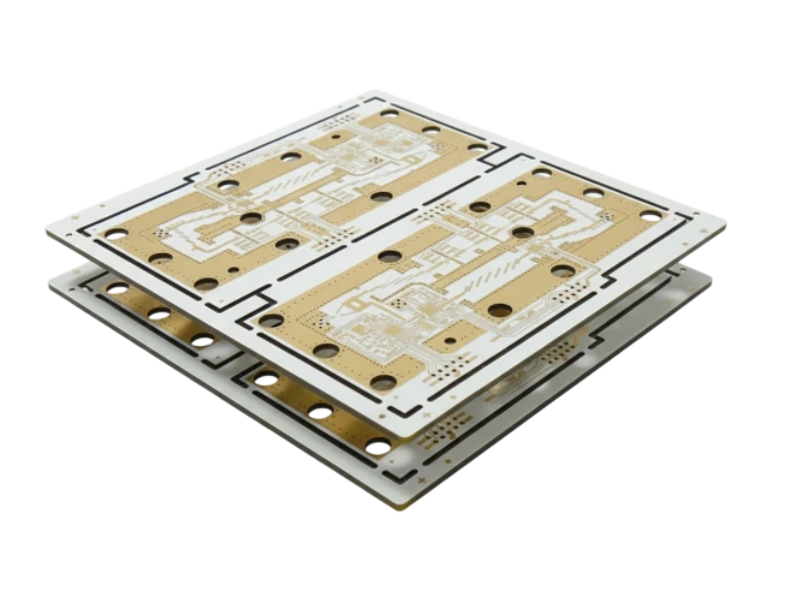
When we discuss a "5G Phone PCB," we are rarely talking about a single board. The architecture of a modern 5G smartphone is a complex ecosystem of interconnected substrates. It generally comprises three distinct categories:
- The Mainboard (SLP/HDI): This is the logic center, housing the AP (Application Processor) and PMIC. In 5G devices, this has evolved into Substrate-Like PCB (SLP) technology. Unlike standard HDI PCB, SLP allows for line widths/spacings (L/S) as low as 30/30μm or even 25/25μm, enabling the density required to fit larger batteries and complex RF front-ends into slim enclosures.
- RF Modules & Antenna-in-Package (AiP): 5G, particularly mmWave (24GHz+), cannot travel long distances over copper traces without massive signal loss. Therefore, the RF transceivers and antennas are integrated into compact modules (AiP) placed at the device's edges. These require specialized high-frequency laminates (Rogers, Tachyon, or LCP).
- Flexible Interconnects (LCP/MPI): Connecting the mainboard to these distributed antenna modules requires flexible PCBs that act as transmission lines. Liquid Crystal Polymer (LCP) and Modified Polyimide (MPI) are the standards here due to their moisture resistance and stable dielectric constants at high frequencies.
The manufacturing distinction is critical: Standard subtractive etching (used in 4G boards) cannot achieve the fine lines required for 5G SLP. We now rely on mSAP (Modified Semi-Additive Process), where copper is built up via plating rather than etched away, ensuring vertical sidewalls and precise impedance control.
Tech Feature → Buyer Impact
| Technical Feature / Decision | Direct Impact (Yield/Reliability) |
|---|---|
| mSAP (Modified Semi-Additive Process) | Enables <30μm trace width. Impact: Increases component density by 40%, allowing larger batteries, but raises fabrication cost by 15-20%. |
| Low Dk/Df Materials (e.g., Megtron 6) | Reduces signal loss at >6GHz. Impact: Directly correlates to 5G data throughput and battery life (less power needed for transmission). |
| Stacked Microvias (Any-Layer) | Allows vertical interconnection between any layers. Impact: Reduces board footprint by up to 30%, essential for folding phones or slim profiles. |
| Thermal Copper Coins / Pastes | Active heat dissipation. Impact: Prevents processor throttling during high-bandwidth 5G downloads. |
Metrics That Matter (How to Evaluate It)
In the 4G era, mechanical reliability was king. In the 5G era, Signal Integrity (SI) and Thermal Integrity share the throne. When evaluating a design or a finished board, these are the non-negotiable KPIs.
| Metric | Typical 4G Value | Required 5G Value | Why It Matters |
|---|---|---|---|
| Dk (Dielectric Constant) | 4.2 - 4.5 (Standard FR4) | 3.0 - 3.6 (Low Loss) | Lower Dk increases signal propagation speed and reduces capacitive coupling (crosstalk). |
| Df (Dissipation Factor) | 0.015 - 0.020 | < 0.005 (Ultra Low Loss) | Critical for mmWave. High Df turns signal energy into heat, killing range and battery. |
| Trace Width / Space | 75μm / 75μm | 30μm / 30μm (SLP) | Essential for routing high pin-count 5G modems and APs in limited space. |
| Impedance Tolerance | ±10% | ±5% or ±7% | Tighter control is needed to prevent signal reflection at high frequencies. |
| Thermal Conductivity | 0.3 - 0.5 W/mK | > 0.8 W/mK (or Hybrid) | 5G chips run hot. The PCB must act as a heatsink to spread heat to the chassis. |
| Moisture Absorption | < 0.5% | < 0.1% (LCP/PTFE) | Water is polar and absorbs RF energy. High absorption destabilizes impedance in humid environments. |
How to Choose (Material & Design Selection)
Selecting the right foundation for your 5G Phone PCB is a balancing act between electrical performance, manufacturability, and cost.
1. Material Selection Strategy
You cannot use standard FR4 for the entire stackup of a 5G device. However, using full Rogers/Teflon stacks is cost-prohibitive for consumer electronics. The industry standard solution is the Hybrid Stackup.
- High-Speed Layers: Use materials like Panasonic Megtron 6/7, Isola I-Tera MT40, or specialized High Frequency PCB laminates for the layers carrying RF signals.
- Digital/Power Layers: Use standard High-Tg FR4 for layers that only handle power distribution or low-speed control signals.
- Bonding Sheets: Low-flow prepregs are essential to prevent resin from flowing into cavities or affecting the impedance of adjacent layers.
2. Design for Signal Integrity
At mmWave frequencies, the "skin effect" becomes dominant. The current flows only on the outer skin of the copper conductor.
- Surface Roughness: You must specify HVLP (Hyper Very Low Profile) copper foil. Standard copper roughness acts like "speed bumps" for high-frequency signals, increasing insertion loss.
- Backdrilling: Stubs in vias act as antennas, causing resonance and signal reflection. Backdrilling (removing the unused portion of the plated through-hole) is mandatory for high-speed lines >10Gbps.
3. Thermal Management
5G modems generate significant heat.
- Structure: Use "Any-layer" HDI designs to create direct thermal paths from the component to the inner ground planes.
- Materials: Consider embedding copper coins or using conductive pastes in vias directly under the PMIC and PA (Power Amplifier).
Implementation Checkpoints (from Design to Fab)
Taking a 5G PCB from a CAD file to a mass-produced unit involves navigating specific risks at each stage. At APTPCB, we utilize a gated process to ensure compliance.
Implementation Roadmap
From Concept to Production
Before CAM work begins, we simulate the stackup using field solvers (like Polar Si9000). We verify that the hybrid materials (FR4 + Low Loss) are compatible regarding CTE (Coefficient of Thermal Expansion) to prevent delamination during reflow.
For trace widths <40μm, we bypass traditional film exposure. We use Laser Direct Imaging (LDI) for high precision. The mSAP process builds copper up on a thin seed layer, ensuring vertical sidewalls for optimal RF performance.
5G boards often use 10-14 layers with stacked microvias. Registration accuracy is critical. We use X-ray drilling targets to align layers dynamically, compensating for any material scaling during lamination.
Final QC goes beyond connectivity. We perform TDR (Time Domain Reflectometry) testing on coupons to verify impedance. For high-end RF boards, we may also test for Passive Intermodulation (PIM) to ensure signal purity.
Common Mistakes (and How to Avoid Them)
Even experienced engineers can stumble when moving to 5G architectures. Here are the most frequent pitfalls we see at APTPCB:
Ignoring the "Fiber Weave Effect": In high-speed signals, if a trace runs parallel to the glass weave of the PCB material, it can experience periodic impedance variations (the "skew" effect).
- Fix: Use "spread glass" fabrics (like 1067 or 1078) or route traces at a slight angle (zig-zag routing) relative to the weave.
Underestimating CTE Mismatch in Hybrid Stacks: Mixing Rogers material (low CTE) with standard FR4 (higher CTE) can cause the board to warp or vias to crack during the high heat of lead-free soldering.
- Fix: Consult with your fab house early. We can recommend compatible prepregs that act as a buffer between disparate core materials.
Over-Specifying Materials: Not every layer needs to be Megtron 7. Using expensive materials on power planes is a waste of budget.
- Fix: Optimize the stackup. Keep high-speed signals on specific layers and use standard materials elsewhere.
Neglecting Surface Finish Impact: ENIG (Electroless Nickel Immersion Gold) is popular, but the nickel layer is magnetic and can cause insertion loss at high frequencies.
- Fix: For 5G RF traces, consider ISIG (Immersion Silver) or ENEPIG, which offer better skin-effect performance.
Supplier Qualification Checklist: How to Vet Your Fab
Before trusting a manufacturer with your 5G design, ask these specific technical questions. A "yes" to all is the minimum requirement for high-reliability production.
- Do you have in-house LDI (Laser Direct Imaging) capabilities? (Essential for <50μm traces).
- Can you demonstrate experience with mSAP or SAP technology? (Required for SLP designs).
- Do you have a dedicated lamination cycle for hybrid stackups? (To manage different cure rates of materials).
- What is your standard impedance tolerance? (Should be ±5% to ±7% for 5G).
- Do you perform cross-section analysis on every production batch? (To verify microvia integrity and plating thickness).
- Do you stock high-frequency laminates (Rogers, Panasonic, Isola)? (Ensures supply chain stability).
- Is your X-Ray inspection capable of checking stacked microvias? (Crucial for Any-layer HDI).
Glossary
mSAP (Modified Semi-Additive Process): A PCB manufacturing method where copper is plated onto a thin seed layer to form traces, rather than etching copper away. This allows for much finer, rectangular traces compared to traditional subtractive etching.
SLP (Substrate-Like PCB): A class of PCB that bridges the gap between traditional circuit boards and IC substrates. It features extremely high density and fine line widths/spacing (typically <30μm).
Dk (Dielectric Constant): A measure of a material's ability to store electrical energy in an electric field. For 5G, a lower and stable Dk is preferred to maximize signal speed.
Df (Dissipation Factor): A measure of how much signal energy is lost as heat within the PCB material. Lower Df is critical for maintaining signal strength in 5G applications.
MIMO (Multiple Input Multiple Output): An antenna technology used in 5G where multiple antennas are used at both the source and the destination. This requires complex PCB routing to support multiple RF chains.
6 Essential Rules for 5G Phone PCB (Cheat Sheet)
| Golden Rule | Why It Matters | Implementation Key |
|---|---|---|
| 1. Prioritize Low Df | Prevents signal loss at mmWave. | Use materials with Df < 0.005. |
| 2. Use mSAP for Density | Enables <30μm traces for SLP. | Verify fab capability for SAP/mSAP. |
| 3. Balance the Stackup | Prevents warpage during reflow. | Symmetric copper distribution. |
| 4. Thermal Vias are Mandatory | 5G chips run extremely hot. | Place directly under PMIC/PA pads. |
| 5. Simulate Impedance Early | Avoids costly re-spins. | Use Polar Si9000 before layout. |
| 6. Watch the Surface Finish | Nickel can cause signal loss. | Prefer Immersion Silver or OSP for RF. |
FAQ
Q: What is the main difference between 4G and 5G PCB manufacturing?
A: The primary difference lies in the density and material requirements. 5G PCBs utilize Substrate-Like PCB (SLP) technology with trace widths under 30μm (requiring mSAP processes) and incorporate ultra-low-loss materials to handle mmWave frequencies, whereas 4G boards typically use standard HDI with subtractive etching and standard FR4.
Q: Why is "Hybrid Stackup" recommended for 5G phones?
A: A hybrid stackup balances performance and cost. High-frequency materials (like Rogers or Megtron) are expensive and are only used on layers carrying RF signals. Standard FR4 is used for power and digital layers to keep the overall board cost viable for mass production.
Q: How does APTPCB handle the thermal challenges of 5G PCBs?
A: We employ several strategies, including the use of high-thermal-conductivity laminates, embedding copper coins directly into the PCB, and utilizing dense arrays of copper-filled thermal vias. Our PCB Assembly process also ensures void-free soldering on thermal pads to maximize heat transfer.
Q: What is the lead time for a 5G SLP prototype?
A: Due to the complexity of mSAP processing and lamination cycles, 5G SLP prototypes typically take 10-15 working days. However, standard HDI boards for 5G applications can often be produced in 5-8 days depending on layer count and material availability.
Q: Can I use standard ENIG finish for 5G boards?
A: While ENIG is reliable, the nickel layer can introduce insertion loss at very high frequencies (mmWave) due to the skin effect. For critical RF traces, we often recommend Immersion Silver, ENEPIG, or OSP, which have better high-frequency characteristics.
Q: Do you support Antenna-in-Package (AiP) substrate manufacturing?
A: Yes, we have capabilities for IC substrate manufacturing and AiP modules, utilizing advanced BT and ABF materials with fine-pitch flip-chip bonding pads to support integrated 5G antenna modules.
Request a Quote / DFM Review for 5G Phone PCB
Ready to move your 5G design from concept to reality? Our engineering team is ready to review your stackup and provide a comprehensive DFM report.
- Gerber Files (RS-274X or ODB++): Ensure all layers are clear.
- Fabrication Drawing: Specify material requirements (e.g., "Panasonic Megtron 6 or equivalent").
- Stackup Diagram: Indicate high-speed layers and impedance requirements.
- Drill Chart: Clearly define blind/buried via structures.
- Quantities: Prototype vs. Mass Production estimates.
Conclusion
The "5G Phone PCB" represents the pinnacle of modern interconnect technology. It is a convergence of material science, thermal engineering, and nanometer-precision manufacturing. Success in this arena requires more than just a vendor; it requires a partner who understands the physics of high-frequency signals and the realities of mass production.
At APTPCB, we have optimized our lines for the 5G era, from mSAP capabilities to rigorous impedance control. Whether you are building a flagship smartphone, an industrial 5G router, or an IoT gateway, our team is equipped to deliver boards that perform.
Contact us today to discuss your project, or explore our High Frequency PCB capabilities to learn more about how we power the next generation of connectivity.