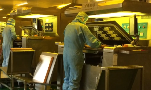
Designing a 5G Small Cell PCB requires navigating a complex intersection of high-frequency signal integrity, compact thermal management, and manufacturability. Unlike traditional macro base stations, small cells (including Femto, Pico, and Micro cells) operate in constrained environments where heat dissipation and signal loss are critical failure points. APTPCB (APTPCB PCB Factory) specializes in fabricating these high-performance boards, ensuring that strict RF specifications are met for both Sub-6GHz and mmWave deployments.
Quick Answer (30 seconds)
For a successful 5G Small Cell PCB build, engineers must prioritize low-loss materials and thermal efficiency.
- Material Selection: Use high-frequency laminates (Rogers, Taconic, or Panasonic Megtron 6/7) with Df < 0.003 and stable Dk over wide frequency ranges.
- Stackup Strategy: Implement hybrid stackups (FR4 + High-Frequency material) to balance cost and RF performance.
- Thermal Management: Integrate copper coins, heavy copper layers (2oz+), or dense thermal via arrays under PA (Power Amplifier) components.
- Impedance Control: Maintain strict ±5% or ±7% tolerance on RF lines; standard ±10% is often insufficient for 5G mmWave.
- Surface Finish: Prefer ENIG or ENEPIG to ensure flat surfaces for fine-pitch components and wire bonding, avoiding HASL due to unevenness.
- PIM Mitigation: Minimize Passive Intermodulation by using low-profile copper foil (VLP/HVLP) and limiting solder mask over high-frequency traces.
When 5G Small Cell PCB applies (and when it doesn’t)
Understanding the specific deployment scenario is crucial before finalizing the PCB architecture. Small cells bridge the gap between massive macro towers and end-user devices.
When to use 5G Small Cell PCB technology:
- High-Density Urban Areas: When network capacity needs to be increased in stadiums, shopping malls, or city centers where 5G Macro Cell PCB infrastructure cannot penetrate or handle the load.
- mmWave Deployment: For short-range, high-bandwidth applications (24 GHz and above) requiring specialized substrates to minimize signal attenuation.
- Indoor Coverage: Enterprise environments requiring dedicated 5G Femto Cell PCB or 5G Pico Cell PCB units to ensure consistent signal through walls.
- Gap Filling: To eliminate dead zones at the edge of a macro cell's coverage area.
- Low Latency Applications: Industrial IoT (IIoT) setups where processing needs to happen closer to the user (Edge Computing).
When it might not be the right fit:
- Wide Area Rural Coverage: A standard 5G Macro Cell PCB is more cost-effective for covering large, sparsely populated geographic areas.
- Low-Frequency IoT Only: If the device only transmits sporadic data packets on NB-IoT or LoRaWAN frequencies (sub-1GHz) without high throughput requirements, standard FR4 boards are sufficient.
- Extremely Low-Cost Consumer Electronics: The materials required for 5G small cells (PTFE, Ceramic-filled hydrocarbons) are significantly more expensive than standard epoxy glass.
- Passive Repeaters: If the device does not process signals but only reflects them, a full active PCB stackup may be unnecessary.
Rules & specifications
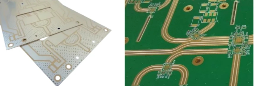
To ensure the reliability of a 5G Small Cell PCB, specific design rules must be adhered to. Deviating from these values often leads to signal degradation or thermal failure.
| Rule | Recommended Value/Range | Why it matters | How to verify | If ignored |
|---|---|---|---|---|
| Dielectric Constant (Dk) | 3.0 – 3.5 (Stable) | Lower Dk reduces signal propagation delay; stability ensures consistent impedance across frequencies. | Review datasheet vs. frequency graphs. | Signal timing errors and impedance mismatches. |
| Dissipation Factor (Df) | < 0.003 @ 10GHz | Minimizes signal loss (insertion loss) which is critical for power efficiency in small cells. | Vector Network Analyzer (VNA) testing on coupons. | High signal attenuation; reduced range; overheating. |
| Copper Roughness | < 2 µm (VLP/HVLP) | Skin effect at 5G frequencies forces current to the surface; rough copper increases resistance and loss. | SEM analysis or spec sheet verification. | Increased insertion loss and phase distortion. |
| Impedance Tolerance | ±5% (RF), ±10% (Digital) | Matches transmission lines to source/load to prevent reflections (VSWR). | Impedance Calculator & TDR testing. | High return loss; signal reflection; reduced data rates. |
| Thermal Conductivity | > 0.5 W/mK (Dielectric) | Small cells are enclosed; the PCB itself must dissipate heat from active components. | Thermal simulation (CFD) software. | Component overheating; throttling; device failure. |
| Via Aspect Ratio | < 8:1 (Through), < 0.8:1 (Micro) | Ensures reliable plating and connectivity in high-layer-count HDI boards. | Cross-section analysis (microsection). | Open circuits; barrel cracks during reflow; unreliable vias. |
| Solder Mask Web | > 3 mil (0.076mm) | Prevents solder bridging between fine-pitch pads common in RF modules. | DFM check in CAM software. | Short circuits during assembly; lower yield. |
| Peel Strength | > 0.8 N/mm | High-frequency materials (PTFE) often have poor adhesion; critical for reliability. | Peel test per IPC-TM-650. | Pad lifting during rework or thermal cycling; delamination. |
| Layer Registration | ± 3 mil | Misalignment affects coupling between layers in RF structures (e.g., broadside coupled lines). | X-ray inspection. | Unpredictable RF performance; impedance variance. |
| Moisture Absorption | < 0.1% | Water is polar and absorbs RF energy; high absorption changes Dk/Df. | Environmental chamber testing. | Performance drift in humid environments; delamination. |
Implementation steps

Moving from specifications to a physical board requires a disciplined workflow. Following these steps ensures the 5G Small Cell PCB meets both electrical and mechanical requirements.
Define Frequency Bands & Architecture
- Action: Determine if the design is Sub-6GHz, mmWave, or both.
- Key Parameter: Operating Frequency (e.g., 3.5 GHz vs. 28 GHz).
- Acceptance Check: Block diagram confirmed with RF engineering team.
Material Selection & Stackup Design
- Action: Select a laminate based on loss budget. For mmWave, choose Rogers or Taconic materials. For cost-sensitive Sub-6GHz, consider Megtron 6.
- Key Parameter: Df value and CTE (Coefficient of Thermal Expansion).
- Acceptance Check: Stackup simulation shows impedance targets are achievable with standard prepreg thicknesses.
Thermal Strategy Planning
- Action: Identify high-power components (PAs, FPGAs) and plan heat dissipation paths. Decide between thermal vias, copper coins, or metal-backed PCBs.
- Key Parameter: Junction-to-Ambient thermal resistance.
- Acceptance Check: Thermal simulation confirms max junction temperature stays below 100°C (or component limit).
Layout & RF Routing
- Action: Route RF lines first. Keep traces short and direct. Avoid 90-degree bends; use 45-degree or curved routing to minimize reflections.
- Key Parameter: Trace width and gap (calculated for 50Ω).
- Acceptance Check: DRC (Design Rule Check) passes for minimum spacing and trace width.
Grounding & Shielding
- Action: Place stitching vias along RF traces (via fencing) to contain fields. Ensure solid ground planes are not broken under RF lines.
- Key Parameter: Via spacing (< λ/20 of highest frequency).
- Acceptance Check: No return path discontinuities found in simulation.
DFM & Prototyping
- Action: Run a DFM Guideline check to ensure the design is manufacturable by APTPCB.
- Key Parameter: Minimum drill size, annular ring, and track/gap.
- Acceptance Check: Clean CAM report with no critical manufacturing violations.
Fabrication & Testing
- Action: Send Gerber files for fabrication. Request TDR (Time Domain Reflectometry) reports.
- Key Parameter: Impedance tolerance verification.
- Acceptance Check: Physical boards pass visual inspection and TDR impedance tests.
Failure modes & troubleshooting
Even with rigorous design, issues can arise during testing or deployment. Here is how to troubleshoot common 5G Small Cell PCB failures.
1. High Insertion Loss (Signal Attenuation)
- Symptom: Signal strength is lower than calculated at the output; reduced range.
- Causes: Wrong material (high Df), rough copper foil, solder mask over RF traces.
- Checks: Verify material batch data; check if solder mask was removed from RF lines (solder mask adds loss).
- Fix: Respin with VLP copper or lower Df material; remove solder mask from high-speed traces.
- Prevention: Specify "Solder Mask Opening" over RF traces in fabrication notes.
2. Passive Intermodulation (PIM)
- Symptom: Noise floor rises; interference in receive bands; reduced data throughput.
- Causes: Ferromagnetic materials (Nickel) in signal path, poor solder joints, rusty connectors, rough copper.
- Checks: PIM testing; inspect surface finish (ENIG can cause PIM due to Nickel; Silver or OSP is better for pure RF).
- Fix: Switch surface finish to Immersion Silver or OSP; improve soldering quality.
- Prevention: Avoid nickel-based finishes on high-power RF lines; use PIM-rated connectors.
3. Thermal Shutdown / Overheating
- Symptom: Device reboots randomly or throttles performance after minutes of operation.
- Causes: Insufficient thermal vias, trapped heat in inner layers, poor contact with heatsink.
- Checks: Thermal camera imaging; inspect thermal paste application; check via plating thickness.
- Fix: Add external heatsink; improve airflow.
- Prevention: Design with embedded copper coins or significantly increase thermal via density under PAs.
4. Impedance Mismatch (High VSWR)
- Symptom: Signal reflection, power loss, potential damage to transmitter.
- Causes: Etching variations, incorrect stackup height, dielectric thickness variation.
- Checks: TDR measurement; cross-section analysis of trace width.
- Fix: Tuning matching networks (if possible); otherwise, board scrap.
- Prevention: Request impedance coupons on the panel; specify strict ±5% tolerance.
5. Delamination during Reflow
- Symptom: Bubbling or separation of layers after assembly.
- Causes: Moisture trapped in PCB; CTE mismatch between hybrid materials (e.g., PTFE and FR4).
- Checks: Bake logs; material compatibility charts.
- Fix: None for affected boards.
- Prevention: Bake boards before assembly; use high-Tg materials; ensure hybrid materials have compatible Z-axis CTE.
6. Via Failure (Open Circuit)
- Symptom: Intermittent connectivity, especially after thermal cycling.
- Causes: Barrel cracking due to Z-axis expansion; poor plating quality.
- Checks: Microsection analysis; continuity test.
- Fix: None.
- Prevention: Use materials with low Z-axis CTE; ensure aspect ratio is within manufacturing limits (e.g., < 8:1).
Design decisions
Troubleshooting often reveals that the root cause lies in early design decisions. When planning a 5G Small Cell PCB, engineers face several critical trade-offs.
Hybrid vs. Homogeneous Stackup
- Decision: Should the entire board be high-frequency material, or just the outer layers?
- Impact: A homogeneous PTFE board offers the best electrical performance but is mechanically soft, difficult to process, and expensive. A hybrid stackup (PTFE outer / FR4 inner) reduces cost and improves rigidity but introduces CTE mismatch risks.
- Recommendation: For 5G Micro Cell PCB designs where cost is a factor, use a hybrid approach. For ultra-high-performance mmWave units, a homogeneous or multi-layer fusion bonding approach may be necessary.
HDI vs. Through-Hole
- Decision: Use High Density Interconnect (HDI) with microvias or standard through-holes?
- Impact: 5G chipsets (BGA) often have fine pitches (0.4mm or less) requiring HDI. HDI improves signal integrity by reducing via stubs but increases cost.
- Recommendation: HDI is almost mandatory for modern 5G Small Cell PCB designs to accommodate BGA breakout and minimize parasitic capacitance.
Surface Finish Selection
- Decision: ENIG, ENEPIG, Immersion Silver, or OSP?
- Impact: ENIG is robust but Nickel is magnetic and can cause PIM. Immersion Silver is excellent for RF but tarnishes easily. OSP is cheap and good for RF but has a short shelf life.
- Recommendation: Use Immersion Silver or ENEPIG for high-frequency 5G boards to balance solderability and RF performance.
FAQ
Q1: What is the main difference between a 5G Small Cell PCB and a Macro Cell PCB? A: The primary difference is scale and power. 5G Small Cell PCB designs are compact, lower power, and often require higher density integration (HDI) compared to the large, high-power, modular setup of a 5G Macro Cell PCB.
Q2: Why are hybrid stackups popular for 5G Small Cells? A: They balance cost and performance.
- RF layers use expensive low-loss materials (Rogers/Taconic).
- Digital/Power layers use standard FR4.
- This reduces total material cost while maintaining signal integrity.
Q3: Can I use standard FR4 for 5G Small Cell PCBs? A: Generally, no, especially for the RF path.
- Standard FR4 has a high Df (loss) and unstable Dk at 5G frequencies.
- It may be used for the digital control section or power distribution layers in a hybrid stackup.
Q4: What is the lead time for manufacturing these PCBs? A: Lead times are typically longer than standard boards due to material availability.
- Standard FR4: 3-5 days.
- Hybrid/RF materials: 10-15 days (depending on stock of Rogers/Panasonic materials).
Q5: How do I manage heat in such a small enclosure? A: Aggressive thermal design is required.
- Use copper coins (embedded metal).
- Use metal-core PCBs (MCPCB) for power stages.
- Maximize thermal via arrays.
Q6: What is the difference between Femto, Pico, and Micro Cell PCBs? A: They differ mainly in power output and coverage range.
- 5G Femto Cell PCB: Lowest power (home/office), smallest form factor.
- 5G Pico Cell PCB: Medium power (enterprise/indoor public), slightly larger.
- 5G Micro Cell PCB: Higher power (outdoor urban), ruggedized, largest of the small cells.
Q7: Why is PIM (Passive Intermodulation) a concern? A: PIM creates interference that blocks upload speeds.
- It acts like self-jamming.
- Critical in 5G where bandwidth is maximized.
Q8: Do I need back-drilling for 5G Small Cell PCBs? A: Yes, if using through-hole vias for high-speed signals.
- Back-drilling removes the unused via stub.
- Stubs act as antennas/filters that degrade signal quality at high frequencies.
Q9: What is the preferred copper foil type? A: VLP (Very Low Profile) or HVLP (Hyper Very Low Profile).
- Smoother copper reduces skin effect losses.
- Essential for mmWave efficiency.
Q10: How does APTPCB verify impedance control? A: We use TDR (Time Domain Reflectometry) on test coupons included on the production panel.
- We measure the actual impedance against the design target.
- Reports are provided with shipment.
Q11: Is blind and buried via technology required? A: Often, yes.
- To save space in compact small cells.
- To improve signal integrity by shortening via stubs.
Q12: What is the cost impact of using Rogers material? A: Rogers materials can be 3x-10x the cost of FR4.
- This is why hybrid stackups are used to minimize the volume of expensive material.
Related pages & tools
- Material Data: Rogers PCB Materials
- Design Tool: Impedance Calculator
- Manufacturing Checks: DFM Guidelines
Glossary (key terms)
| Term | Definition | Context in 5G Small Cell PCB |
|---|---|---|
| mmWave | Millimeter Wave (24 GHz - 100 GHz). | Requires ultra-low loss materials and tight tolerances. |
| Sub-6GHz | Frequencies below 6 GHz. | The "coverage" layer of 5G; less demanding than mmWave but harder than 4G. |
| PIM | Passive Intermodulation. | Signal distortion caused by nonlinearities in passive components (connectors, traces). |
| Dk (Dielectric Constant) | Measure of a material's ability to store electrical energy. | Affects impedance and signal propagation speed. |
| Df (Dissipation Factor) | Measure of how much energy is lost as heat in the material. | Lower Df is critical for 5G efficiency. |
| CTE | Coefficient of Thermal Expansion. | How much the material expands with heat; mismatch causes delamination. |
| MIMO | Multiple Input Multiple Output. | Using multiple antennas; increases PCB complexity and routing density. |
| Beamforming | Focusing signal towards a specific user. | Requires precise phase control on the PCB antenna array. |
| Backhaul | The connection from the small cell to the core network. | The PCB must support high-speed fiber or wireless backhaul interfaces. |
| Small Cell | Low-power wireless access points (Femto, Pico, Micro). | The device housing the PCB; used for densification. |
| Hybrid Stackup | Combining different laminate materials. | Used to optimize cost/performance in 5G Small Cell PCB designs. |
Conclusion
Designing a 5G Small Cell PCB is a balancing act between high-frequency performance, thermal endurance, and manufacturing feasibility. Whether you are building a 5G Femto Cell PCB for indoor use or a rugged 5G Micro Cell PCB for outdoor densification, the rules of physics regarding Dk, Df, and thermal dissipation remain absolute.
By adhering to the specifications outlined above—specifically regarding material selection, hybrid stackups, and PIM mitigation—engineers can avoid costly respins and field failures. APTPCB supports this process from prototype to mass production, offering the specialized materials and DFM expertise required for next-generation networks.
For a detailed review of your specific stackup or to get accurate pricing on high-frequency laminates, request a quote today.