Contents
- Highlights
- D0 to D3: The "Emergency Room" Phase
- D4: The Autopsy (Root Cause Analysis)
- D5 to D7: Engineering the Permanent Fix
- Reliability & Future Outlook
- Supplier Qualification Checklist: How to Vet Your Fab
- Glossary
- 6 Essential Rules for 8d Problem Solving PCB (Cheat Sheet)
- FAQ
- Request a Quote / DFM Review for 8d Problem Solving PCB
- Conclusion
It was 4:30 PM on a Friday—the universal time for engineering disasters to strike. My phone buzzed with a frantic call from a Tier-1 automotive client. Their new ECU line, running on our high-reliability HDI boards, had just hit a 15% fallout rate at End-of-Line (EOL) testing. The error? Intermittent open circuits on the CAN bus line. In the world of mass production, this is the equivalent of a five-alarm fire. We didn't just need a quick fix; we needed a forensic investigation. This is where 8d problem solving pcb methodologies transition from boring paperwork to a critical survival tool.
In the context of PCB manufacturing, the 8D (Eight Disciplines) process is a structured problem-solving approach used to identify, correct, and eliminate recurring problems. It is the industry standard—particularly in automotive and aerospace sectors—for turning a chaotic production failure into a controlled, engineered solution. It forces us to move beyond "we fixed it" to "we engineered the process so it physically cannot happen again."
Highlights
- Containment is Not a Cure: Why isolating the "bleeding" (D3) is critical before you even touch a microscope for Root Cause Analysis (RCA).
- The "Ghost" in the Via: How thermal shock and resin smear often disguise themselves as random failures in 8d problem solving pcb scenarios.
- Data Over Opinion: The necessity of cross-section analysis and SEM (Scanning Electron Microscopy) over operator intuition.
- Systemic Prevention: Moving from "retraining the operator" (a weak fix) to "poka-yoke" (error-proofing) the equipment.

D0 to D3: The "Emergency Room" Phase
When that call came in, we immediately initiated D0 (Preparation) and D1 (Team Formation). In PCB manufacturing, you cannot solve a complex plating issue alone. We assembled a team: the Process Engineer (for the chemistry), the CAM Engineer (for the data), and the Quality Manager.
The immediate challenge was D2 (Problem Description). The client reported "open circuits." But "open" is vague. Was it a true open? A high-resistance net? Did it fail at room temperature or only after reflow? We narrowed it down: Intermittent high resistance on Net #402 after second reflow. This precision is vital.
Then came D3: Intermittent Containment Action (ICA). This is the step most junior engineers skip, and it’s fatal. We didn't know why the boards were failing yet, but we had to stop bad boards from reaching the customer's assembly line.
- Action: We implemented a 100% electrical re-test of all stock in the warehouse, specifically stressing Net #402.
- Result: We quarantined 3,000 units. Production didn't stop, but the "bleeding" was contained. At APTPCB, our digital traveler system allows us to instantly lock specific lot numbers in the MES (Manufacturing Execution System), preventing shipping.
D4: The Autopsy (Root Cause Analysis)
This is the heart of 8d problem solving pcb. We took the failing samples to the lab. A standard visual inspection showed nothing—the pads looked perfect. This suggested the failure was internal.
We performed vertical cross-sectioning (micro-sectioning) on the suspect vias. Under the microscope at 200x magnification, we saw the culprit: ICD (Interconnect Defect). There was a hairline separation between the inner layer copper and the plated copper barrel of the via.
Why did this happen? We used the "5 Whys" technique:
- Why? The copper separated.
- Why? There was residue between the layers.
- Why? The desmear process (removing resin smear after drilling) was incomplete.
- Why? The chemical bath activity was low.
- Why? The automatic dosing pump had a calibration drift that wasn't caught by the daily sensor check.
The root cause wasn't "bad copper"; it was a sensor calibration drift in the desmear line. This is why generic "operator error" is rarely the true root cause in complex PCB fabrication processes.
D5 to D7: Engineering the Permanent Fix
Finding the root cause is satisfying, but fixing it permanently (D5/D6) is where the engineering trade-offs happen. We couldn't just "calibrate the pump" and hope for the best. That’s a temporary fix.
We had to choose a Permanent Corrective Action (PCA). We evaluated three options using a decision matrix (see below). The goal was to ensure that even if a pump drifted, the product wouldn't fail.
Engineering Decision Matrix: Corrective Actions for Desmear Failure
| Corrective Action Option | The "Lab" Benefit (Pros) | The "Fab" Reality (Cons/Risks) |
|---|---|---|
| Option A: Increase Manual Titration Frequency | Low cost, immediate implementation. Catches chemistry drift sooner. | Relies on human discipline. High risk of "pencil whipping" (faking logs) during night shifts. |
| Option B: Plasma Cleaning (Secondary Desmear) | Physical removal of resin. Extremely reliable for HDI/Blind vias. | Adds 2 hours to cycle time. High energy cost. Potential bottleneck for mass production. |
| Option C: Automated pH/Redox Controller Interlock | Stops the line automatically if chemistry drifts. Zero human error. | High initial CAPEX. Requires software integration with MES. |
We chose Option B (Plasma Cleaning) as an immediate PCA for the high-reliability automotive batch, while implementing Option C as the long-term D7 (Preventive) measure across the factory. Plasma cleaning physically bombards the via with gas ions, ensuring a clean surface for plating even if the chemical desmear is slightly off. It was a trade-off: we sacrificed some throughput speed for absolute reliability—a necessary choice for automotive electronics PCBs.
Reliability & Future Outlook
The final step of the 8D process involves validation. We didn't just assume the Plasma Clean worked. We ran a new batch (D6 Validation) and subjected it to IST (Interconnect Stress Testing). This cycles the PCB from room temperature to 150°C hundreds of times to simulate years of field use. The result? Zero failures.
The future of 8d problem solving pcb is moving away from reactive autopsies toward predictive analytics.
5-Year Technology Trajectory: From Reactive to Predictive
| Metric | Standard Today | Target Tomorrow | Why it matters |
|---|---|---|---|
| Defect Detection | Post-process AOI/E-Test | In-line AI Monitoring | Catches drift before it becomes a defect. |
| Traceability | Lot/Batch Level | Panel/Unit Level (Laser ID) | Surgical containment of 10 boards instead of 3,000. |
| 8D Cycle Time | 5-10 Days | 24-48 Hours | Minimizes supply chain disruption. |

Supplier Qualification Checklist: How to Vet Your Fab
If you are sourcing PCBs for critical applications, you must ensure your supplier can handle a rigorous 8D process. Ask these questions during your audit:
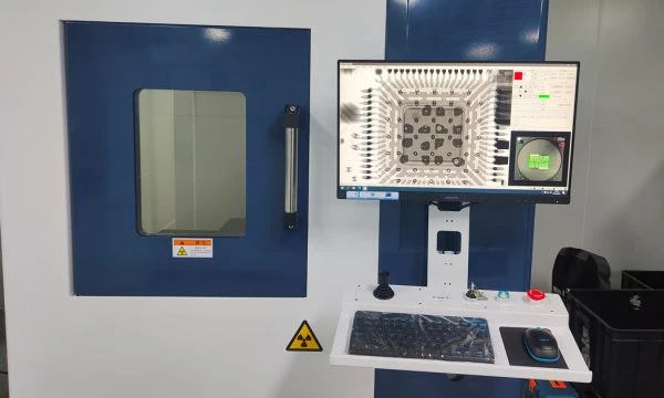
- Does the factory have an in-house failure analysis lab? (Look for Cross-section equipment, SEM, and X-Ray).
- What is your standard retention period for production records? (Automotive requires 15+ years).
- Can you demonstrate a closed 8D report from the last 6 months? (Check if the root cause was "operator error"—if so, it's a red flag).
- Do you use a digital MES (Manufacturing Execution System) for chemical line monitoring?
- What is your procedure for "Interim Containment"? (Do they have a quarantine cage? Is it physically locked?).
- Do you perform reliability testing (Thermal Shock/Solderability) on every batch or just periodically?
Glossary
- 8D (Eight Disciplines): A problem-solving methodology designed to find the root cause of a problem, devise a short-term fix, and implement a long-term solution to prevent recurrence.
- ICA (Interim Containment Action): Temporary steps taken to "stop the bleeding" and protect the customer from defects while the root cause is being investigated.
- PCA (Permanent Corrective Action): The final engineering change (process, tooling, or design) that eliminates the root cause.
- Desmear: A chemical or plasma process used to remove resin residue from the inside of drilled holes to ensure good electrical connection.
- MES (Manufacturing Execution System): Software that tracks and documents the transformation of raw materials to finished goods in real-time.
6 Essential Rules for 8d Problem Solving PCB (Cheat Sheet)
- Contain First, Analyze Later: Never start root cause analysis until you have secured the supply chain (ICA).
- Data > Opinions: "I think it's the drill speed" is a guess. A cross-section photo is data.
- The "5 Whys" is Mandatory: If you stop at "the machine broke," you haven't found the root cause. Ask why it broke.
- Replicate the Failure: If you cannot reproduce the defect in the lab, you haven't found the true root cause.
- Validate the Fix: A PCA is only valid if you can prove it works through stress testing (e.g., PCB Quality Testing).
- Update the FMEA: If a failure occurred that wasn't in your Failure Mode and Effects Analysis, update the document immediately.
FAQ
Q: What is the difference between an 8D Report and an RMA?
A: An RMA (Return Merchandise Authorization) is the logistical process of returning bad goods. An 8D Report is the technical engineering document that explains why the goods were bad and how the factory fixed the process.
Q: How long should an 8D investigation take?
A: Ideally, D0-D3 (Containment) should be done within 24-48 hours. The full D8 closure usually takes 1-2 weeks, depending on the complexity of the validation testing required (e.g., thermal cycling takes time).
Q: Is 8D required for prototype boards?
A: Typically, no. 8D is heavy on process control and is best suited for mass production stability. For prototypes, a simpler "Corrective Action Report" (CAR) is usually sufficient unless the failure is catastrophic.
Q: Can a design issue trigger an 8D?
A: Yes. Sometimes the root cause (D4) reveals that the PCB design itself was not manufacturable (e.g., annular rings too small). In this case, the PCA (D5) is a design revision, not a factory process change.
Q: Why do automotive customers insist on 8D?
A: Automotive electronics have zero tolerance for liability. The 8D format provides a legal and technical audit trail proving that the supplier exercised due diligence in resolving safety-critical failures.
Q: What if the root cause cannot be found?
A: This is called "No Fault Found" (NFF). It is dangerous. In this case, the focus shifts entirely to robust containment (testing screens) until the defect re-appears or is trapped by improved detection methods.
Request a Quote / DFM Review for 8d Problem Solving PCB
To ensure your project benefits from our rigorous quality systems and 8D capabilities, please provide the following when requesting a quote:
- Gerber Files: RS-274X or ODB++ format.
- Fabrication Drawing: Clearly state IPC Class (2 or 3) and any specific reliability testing requirements (e.g., IST, HATS).
- Stackup Details: Copper weight, dielectric thickness, and impedance requirements.
- Quality Requirements: If you require PPAP (Production Part Approval Process) or specific 8D reporting formats, mention this upfront.
- Volume & EAU: Estimated Annual Usage helps us plan the necessary process controls.
- Base Material: FR4, Rogers, Polyimide, etc. (See our Materials Page).
Conclusion
The story of the "Ghost in the Via" taught us that in 8d problem solving pcb, the obvious answer is rarely the correct one. By strictly following the 8D disciplines—containing the mess, digging deep with cross-sections, and implementing automated, permanent fixes—we turned a potential recall into a demonstration of reliability.
At APTPCB, we don't just manufacture boards; we engineer resilience. Whether you are dealing with a simple consumer device or a complex automotive ECU, our commitment to root cause analysis ensures that your production line stays running.
Ready to secure your supply chain? Contact our engineering team today.
