
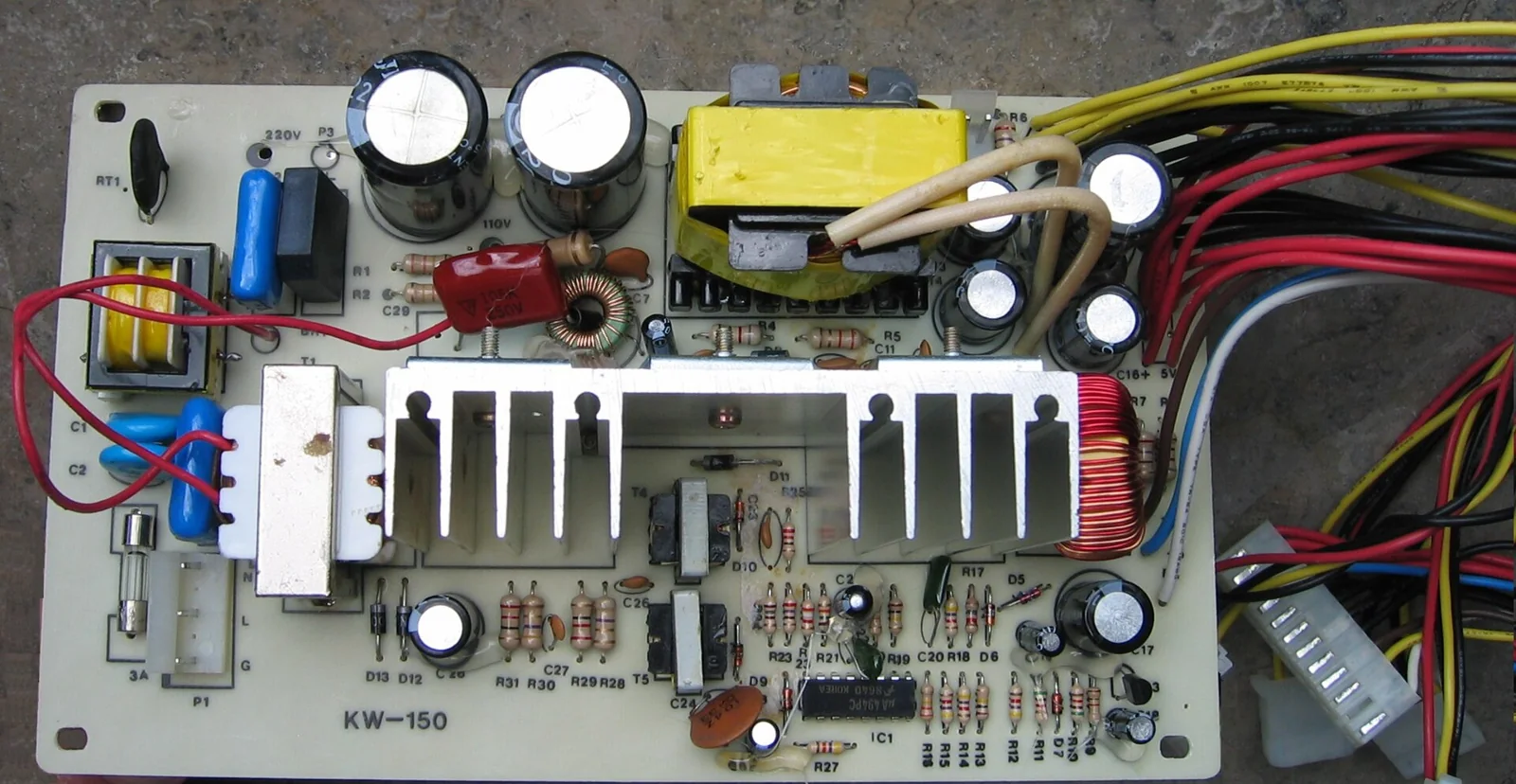
An AC-DC power supply PCB is the board that takes hazardous mains voltage on one edge and has to deliver a clean, safe, low-voltage DC rail on the other. Most design guides explain what a switched-mode supply is. The harder question, and the one that decides whether a prototype survives qualification, is whether the board keeps a sound isolation barrier, a tight switching loop, and a continuous heat path after solder mask, assembly, cleaning, fastening, and coating have all been applied.
This guide treats the AC-DC board as a coupled electrical-thermal-safety subassembly and walks through what to review before release. It does not prove safety certification, insulation acceptance, or efficiency results. Those belong to the finished product and its standards owner, not to a board article.
Quick Answer An
AC-DC power supply PCBis best reviewed as a board split by a live mains-to-SELV isolation barrier, carrying a high-di/dtswitching loop and a concentrated heat source. The practical release question is notDoes the topology work on the bench?It isDoes the isolation gap, the switching loop, and the heat path stay intact after solder mask, placement, cleaning, fastening, and coating are applied to a real panel?
Table of Contents
- What does an AC-DC power supply PCB have to get right?
- Why the mains-side section drives the whole board review
- Where AC-DC board failures start: the isolation barrier under assembly
- A board-level review checklist before release
- Input, PFC, and switching-loop layout: what manufacturability depends on
- Thermal path and copper for continuous mains-powered loads
- What design files make the review useful
- How to get an AC-DC board reviewed before release
- FAQ
- Public references
- Author and review information
What does an AC-DC power supply PCB have to get right?
Start with the physical regions, not the topology label. Whether the design is a flyback, forward, or resonant converter, the board has to keep four areas distinct and review each for a different dominant risk.
| Board region | Dominant board-level risk | What the review confirms |
|---|---|---|
| Mains input and rectification | Surface tracking, inrush, fusing coordination | Live-side copper, fuse and inrush parts, and the start of the isolation boundary are placed before anything else routes around them |
| Power-factor and bulk-storage stage | Hot-loop area, bulk capacitor heat and height | The high-current loop is small and the tall bulk parts do not block airflow or bridge the barrier |
| Isolated conversion stage (transformer + switch) | Isolation gap integrity, switching-node EMI | Primary and secondary copper never approach across the barrier, and the switching loop is tight on one layer |
| Secondary, control, and feedback | Reference contamination, feedback noise pickup | Output rectification, sense, and the opto/feedback crossing sit cleanly and do not pick up switching noise |
The mistake the weakest AC-DC pages make is to treat the board as one flat "power PCB." It is not. The isolation barrier physically divides it into a hazardous-voltage half and a user-accessible half, and almost every serious board-level problem hides at a boundary between these regions rather than inside one block.
For broader construction context, the closest support page is PCB Stack-Up. For application landing context, see Power & Energy PCB and, for control-side product context, Industrial Control PCB.
Why the mains-side section drives the whole board review
On a DC-only board, every net is referenced to a common low voltage and the worst case is signal integrity or a hot component. On an AC-DC board, one edge of the PCB is energized to the full rectified mains potential, and a user can touch the other edge. That single fact reorders the whole review.
The mains side imposes constraints the rest of the board has to respect:
- the live copper, fuse, and inrush components have to be placed and bounded first, because the isolation boundary they start cannot be negotiated later
- creepage and clearance across the primary-to-secondary barrier are set by the working voltage, the pollution degree of the end environment, and the material group of the laminate, all defined by the applicable safety standard — they are inputs the layout must honor, not values a board shop certifies
- the transformer, opto-coupler, and any Y-capacitor are the only parts allowed to cross the barrier, and each of them has its own creepage requirement that the footprint and keep-out must preserve
Because of this, an AC-DC board is closer to a constrained safety subassembly than to a generic converter board. If the barrier is treated as an afterthought, the rest of the review becomes reactive: a slot added here, a component nudged there, a silk warning that nobody enforced on the panel. That is a weak release posture. The barrier should be drawn and locked as a keep-out spanning every layer before the dense routing starts.
Where AC-DC board failures start: the isolation barrier under assembly
The primary mechanism family for this board class is dielectric / surface-insulation breakdown across the isolation barrier, and the thing that makes it dangerous is that the barrier is defined in layout but degraded in manufacturing.
A representative board-level failure chain:
- The layout sizes the primary-to-secondary gap to the working voltage and pollution degree required by the applicable standard, and the dry prototype passes its bench checks.
- Real manufacturing then crowds that gap with things the schematic never showed: a solder-mask sliver or silk bridging the slot, flux residue left after an incomplete clean, a tall heatsink or capacitor body that mechanically spans the barrier, or conformal coating that wicks across and changes the surface condition.
- In the field, humidity, dust, or condensation settles on the weakened surface path and the barrier begins to track — the surface carbonizes into a conductive trace.
- Tracking lowers the surface resistance further, producing leakage current, partial discharge, and eventually flashover across what was supposed to be a safe barrier.
- A board that passed a dry electrical check now fails dielectric-withstand testing, leaks touch current, or breaks down after weeks in service — and the root cause was a manufacturing and assembly interaction at the barrier, not the schematic.
The important point is that the first electrical check can pass while the board is already compromised. A barrier review that only looks at the netlist and not at solder mask, cleaning, component height, and coating behavior is paperwork, not an isolation review.
Side note — the switching loop is the secondary risk. The high-
di/dtloop formed by the bulk capacitor, the switch, and the transformer primary is the other place a clean schematic goes wrong on a real board. A loop with too much enclosed area turns every switching edge into voltage overshoot and radiated noise, which shows up late as conducted-emissions trouble or stressed switch devices. Keep this loop small and on one layer, but review it as a separate, single concern — not folded into the isolation story.
A board-level review checklist before release
Use a staged review keyed to the regions above, instead of asking the board to prove finished-product safety.
| Review question | What to look for | Why it is a release issue |
|---|---|---|
| Is the isolation barrier a locked keep-out on every layer? | No copper, plane, via, mask sliver, or silk crosses the primary-to-secondary gap on any layer | The barrier is the one feature that cannot be fixed after fabrication without a respin |
| Are barrier-crossing parts the only crossings? | Transformer, opto, and Y-cap footprints preserve their own creepage; nothing else bridges | Each crossing component carries its own clearance that placement can quietly violate |
| Is the switching hot loop tight and singular? | Bulk cap, switch, and primary form one small loop on one layer | A large loop converts into overshoot and emissions that surface only in EMC pre-scan |
| Are cleaning and coating compatible with the gap? | Residue, no-clean choice, and coating wicking are reviewed against the barrier surface | A "passing" dry board can track once contamination or coating changes the surface |
| Is the heat path continuous after assembly? | Switch and rectifier route heat through copper, vias, and any heatsink contact without interruption | Thermal intent on paper often changes once parts, fasteners, and enclosure enter |
| Is the validation language at board level? | Review stays on DFM, stackup, placement, inspection, and dielectric/functional test planning | The board release must not be read as product safety certification or efficiency proof |
If the release package still needs stackup or manufacturing-note cleanup, the companion resource is DFM Guidelines. For inspection and test-planning language, the closest support page is Testing & Quality.
Input, PFC, and switching-loop layout: what manufacturability depends on
The input and power-factor stages are where current is highest and where layout decisions turn into manufacturability and EMC outcomes.
Input and rectification. Full-bridge rectification feeds the bulk storage and, where required, a power-factor stage. Inrush limiting (commonly an NTC or an active limiter) and the input fuse have to be coordinated and placed so the live copper stays bounded by the isolation keep-out from the start. Universal-input designs that accept roughly the worldwide mains range concentrate the widest current swing here, so the copper and the loop geometry, not the schematic, set the real behavior.
Power-factor correction. Regions that require power-factor correction add a boost stage and a high-voltage bulk bus. Power-factor and harmonic limits are defined by the applicable regional regulation (for example the IEC 61000-3-2 family), and conducted-emissions behavior is judged against the relevant EMC standard (for example the EN 55032 / CISPR family). A board review does not prove compliance with any of these; it confirms that the layout gives the design a fair chance — tight loops, sane filter placement, and a return path that does not force common-mode current across the barrier.
Switching loop and feedback. Keep the primary switching loop small and on a single layer, place the gate and sense returns with a Kelvin-style connection to avoid power current corrupting the control reference, and route the feedback or opto path away from the switching node so it does not pick up dV/dt noise. These are layout disciplines that a multilayer PCB stackup with a solid reference plane makes far easier to achieve than a two-layer board can.
The reason these belong in a board review and not just a schematic review is that all three depend on physical geometry — loop area, plane continuity, and component placement — that only exists once the board is laid out on a real stackup.
Thermal path and copper for continuous mains-powered loads
AC-DC supplies usually run continuously, so the switch, the rectifier, and the magnetics sit at a steady elevated temperature rather than a transient one. The board-level review question is whether heat can leave those parts through copper, vias, and any heatsink or chassis contact without being interrupted by the assembly.
Practical review points:
- concentrate spreading copper under the switch and output rectifier, and use a heavy copper PCB build where the current and heat justify it
- use thermal-via fields to move heat to an opposite-side pour or a mechanical heatsink, and check that solder-mask and paste choices keep those vias effective rather than wicking paste away from the joint
- where a metal heatsink or enclosure wall is the real cooling path, treat its contact as part of the board review — flatness, fastener torque, and interface material decide whether the nominal thermal path survives fastening
- for high ambient or sealed-enclosure designs, a high thermal conductivity PCB or metal core PCB construction can change the whole thermal strategy, and that choice should be made during the board review, not after the first hot prototype
The lane-specific caution: a board review can show that the heat path is continuous; it cannot promise a finished thermal-rise number, an efficiency figure, or a service-life rating. Those are product-level results that depend on the enclosure, the load profile, and the qualification program.
What design files make the review useful
An AC-DC board review is only as good as the package it is given. The barrier, the loop, and the heat path are physical, so the inputs have to expose physical intent, not just connectivity.
The most useful inputs are:
- fabrication data with the intended stackup and the laminate material group, because creepage depends on it
- placement data that makes the mains, isolation, conversion, and control zones easy to read
- the marked isolation boundary and any required slot or keep-out, so the barrier can be checked against every layer
- BOM context for the barrier-crossing parts (transformer, opto, Y-cap) and the main thermal components
- mechanical references for any heatsink, chassis, or enclosure contact and the intended fastening
- notes on cleaning process, no-clean vs. wash, and conformal coating, because all three interact with the barrier surface
Without those, a board team can comment on broad manufacturability but cannot speak to the real AC-DC release problem: whether the isolation barrier and heat path still exist after the board is built.
How to get an AC-DC board reviewed before release
If you are taking an AC-DC power supply board toward qualification and you are not fully certain that the isolation barrier, the switching loop, and the heat path all survive your actual manufacturing process, a board-level review is worth running before you commit to a build.
Send your Gerber or ODB++, the intended stackup and laminate material group, placement data with the isolation boundary marked, BOM context for the barrier-crossing and thermal parts, and any mechanical references for heatsink or enclosure contact to [email protected] or through the AC-DC power supply PCB review request.
APTPCB's power-board engineering team returns a board-level review covering: where the isolation keep-out is violated on any layer, where the switching loop area is larger than it needs to be, where cleaning or coating choices threaten the barrier surface, and where the heat path is interrupted by copper balance, vias, or mounting. The review stays at the board boundary — it identifies manufacturability and release risks; it does not certify product safety, EMC, or efficiency.
Related paths:
FAQ
Does an AC-DC power supply PCB article prove safety compliance?
No. A board-level review can explain how to keep the isolation barrier, switching loop, and heat path intact, but it does not prove product safety certification, dielectric acceptance, or any standards compliance. Those belong to the finished product and its certifying body.
Why is the isolation barrier the first thing to review?
Because it is the one feature that physically divides hazardous mains voltage from the user-accessible side, and it cannot be repaired after fabrication without a respin. Locking it as a keep-out on every layer before dense routing starts prevents the most common and most serious AC-DC board failures.
Why can a board pass a bench test and still fail in the field?
Early electrical checks run on a clean, dry board. Field failures usually come from the isolation surface degrading — flux residue, a mask sliver, a part bridging the gap, or coating wicking — which only tracks and breaks down once humidity, dust, or condensation arrives. The review has to look at manufacturing and surface condition, not just the netlist.
How big should the switching loop be?
As small as the parts allow, kept on a single layer with the bulk capacitor, switch, and transformer primary close together. The exact geometry depends on the devices and stackup, so the review goal is to minimize the enclosed loop area rather than hit a universal number.
Should creepage and clearance numbers come from the blog?
No. Creepage and clearance are set by working voltage, pollution degree, material group, and the applicable safety standard for the end product. They are inputs to the layout review, not values a board shop publishes as a guarantee.
What package makes the review most useful?
Fabrication data with stackup and material group, placement with the isolation boundary marked, BOM context for the barrier-crossing and thermal parts, and mechanical references for heatsink or enclosure contact. That combination lets the review check the barrier, the loop, and the heat path as they will actually be built.
Public references
PCB Stack-Up Support-page context for stackup definition and controlled construction planning.
Power & Energy PCB Application-page context for converter, charger, and power-board manufacturing scope.
Heavy Copper PCB Support-page context for high-current copper and thermal-spreading construction.
DFM Guidelines Support-page context for manufacturing review intake and pre-release clarification.
Testing & Quality Support-page context for inspection, dielectric, and functional test-planning language at board level.
Author and review information
- Author: APTPCB editorial team
- Technical review: Power electronics PCB engineering review team
- Review scope: Board-level isolation barrier, switching-loop layout, heat path, manufacturability, and release-boundary consistency