Quick Answer (30 seconds)
Successful ADAS radar PCB layout for 24GHz and 77GHz automotive systems requires strict control over material properties and geometric tolerances. Unlike standard digital boards, millimeter-wave (mmWave) radar designs function as part of the antenna system itself.
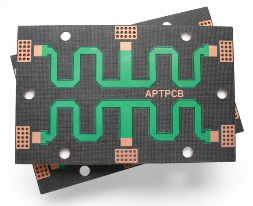
- Material Selection: Use high-frequency laminates (e.g., Rogers RO3003, RO4835) with extremely low Dielectric Constant (Dk) and Dissipation Factor (Df).
- Stackup Strategy: Implement hybrid stackups (High-frequency material on top, FR4 for digital/power layers) to balance performance and cost.
- Etching Precision: Line width tolerances must be controlled within ±15μm (or tighter) to maintain impedance and antenna gain.
- Grounding: Use extensive via stitching around RF lines (Grounded Coplanar Waveguide) to suppress surface waves and prevent crosstalk.
- Surface Finish: Prefer Immersion Silver or ENIG for flat surfaces; avoid HASL due to uneven thickness affecting signal propagation.
- Thermal Management: Direct thermal vias under MMIC (Monolithic Microwave Integrated Circuit) components are mandatory for heat dissipation in enclosed radar modules.
When ADAS radar PCB layout applies (and when it doesn’t)
Understanding the specific domain of mmWave radar ensures you apply the correct design rules.
This guide applies to:
- 77GHz Long-Range Radar (LRR): Adaptive Cruise Control (ACC) and Automatic Emergency Braking (AEB) systems.
- 24GHz Short/Mid-Range Radar (SRR/MRR): Blind spot detection, cross-traffic alert, and parking assistance.
- 4D Imaging Radar: High-resolution sensor arrays requiring complex antenna structures and HDI techniques.
- Hybrid PCB Designs: Boards combining RF front-ends with digital processing units (DSP/MCU) on a single panel.
This guide does not apply to:
- Ultrasonic Sensors: These operate at sound frequencies (kHz) and use standard FR4 layouts.
- LiDAR Systems: While optical, the PCB layout focuses more on high-speed digital and laser driver pulses rather than RF wave propagation.
- Standard Camera Modules: Focus here is on MIPI CSI-2 high-speed differential pairs, not mmWave antenna structures.
- General Automotive ECUs: Body control modules or infotainment systems do not require the exotic materials or etching tolerances of radar.
Rules & specifications
The following table outlines the critical parameters for ADAS radar PCB layout. Deviating from these rules often leads to signal attenuation or ghost targets.
| Rule | Recommended Value/Range | Why it matters | How to verify | If ignored |
|---|---|---|---|---|
| Dielectric Constant (Dk) Stability | Dk ±0.05 tolerance | Variations shift the center frequency of the antenna. | Review material datasheet & batch certs. | Radar frequency drift; reduced range. |
| Dissipation Factor (Df) | < 0.002 @ 77GHz | High Df causes signal energy loss as heat. | Select PTFE or ceramic-filled hydrocarbon. | Significant signal loss; reduced detection distance. |
| Copper Roughness | VLP or HVLP (< 1μm Rz) | Skin effect at 77GHz makes current flow on surface; roughness increases resistance. | SEM analysis or specify foil type in Fab Note. | Increased insertion loss; poor signal integrity. |
| Etch Tolerance | ±15μm (0.5 mil) | Antenna patch dimensions define the resonant frequency. | AOI (Automated Optical Inspection). | Antenna mismatch; lower gain. |
| Solder Mask on RF Lines | Remove (Open) | Solder mask has high Df and variable thickness, altering impedance. | Gerber viewer check (Soldermask layer). | Unpredictable impedance shifts; signal loss. |
| Via Stitching Pitch | < λ/8 (approx. 0.4mm at 77GHz) | Prevents substrate integrated waveguide (SIW) leakage. | DRC (Design Rule Check) in CAD. | EMI leakage; crosstalk between channels. |
| Surface Finish | Immersion Silver / ENIG | Requires flat surface for fine-pitch components and skin effect. | X-Ray Fluorescence (XRF) for thickness. | Signal reflection; poor solder joints on MMICs. |
| Registration Accuracy | ±50μm (Layer to Layer) | Misalignment between antenna layer and ground plane affects coupling. | X-Ray drill check. | Asymmetric beam patterns. |
| Thermal Via Plugging | Conductive/Non-conductive fill + Cap | Prevents solder wicking from MMIC thermal pads. | Cross-section analysis. | MMIC overheating; reliability failure. |
| Glass Weave Style | Spread Glass (e.g., 1067, 1078) | Prevents "fiber weave effect" where traces see different Dk. | Specify glass style in stackup. | Skew in differential pairs; signal distortion. |
Implementation steps

Designing an ADAS radar PCB layout requires a systematic approach that integrates electrical performance with manufacturability.
Define the Hybrid Stackup
- Action: Select a high-frequency laminate (e.g., Rogers RO3003) for the top layer (L1-L2) and standard FR4 for lower layers.
- Key Parameter: CTE (Coefficient of Thermal Expansion) matching between materials.
- Acceptance Check: Verify the manufacturer's ability to bond dissimilar materials without delamination.
Calculate Impedance and Line Widths
- Action: Use a field solver to calculate trace widths for 50Ω transmission lines, accounting for the lack of solder mask.
- Key Parameter: Copper thickness (usually 0.5 oz or 1 oz rolled copper).
- Acceptance Check: Simulation results match the target impedance within ±5%.
Place MMIC and Antenna Array
- Action: Place the Radar Transceiver (MMIC) centrally to minimize trace length to the antennas.
- Key Parameter: Shortest possible RF path.
- Acceptance Check: No crossing of RF lines; direct routing to patch antennas.
Route Grounded Coplanar Waveguides (GCPW)
- Action: Route RF signals with ground pour on the same layer, stitched to the reference plane below.
- Key Parameter: Gap distance between trace and top-layer ground.
- Acceptance Check: Via fencing is continuous along the entire RF path.
Implement Thermal Management
- Action: Place a dense array of thermal vias directly under the MMIC exposed pad.
- Key Parameter: Via diameter (typically 0.2mm - 0.3mm) and plating thickness.
- Acceptance Check: Thermal simulation confirms junction temperature stays below limit (e.g., 125°C).
Apply Solder Mask Keep-Outs
- Action: Define keep-out areas over all high-frequency traces and antenna patches.
- Key Parameter: Clearance margin (typically 100μm larger than the trace).
- Acceptance Check: Visual verification that no mask covers the RF conductors.
Final DFM & Etch Compensation
- Action: Adjust trace widths in the manufacturing files to account for etch factors (etch compensation).
- Key Parameter: Etch factor provided by APTPCB (APTPCB PCB Factory).
- Acceptance Check: Final Gerber geometry aligns with the nominal design requirement after etching.
Failure modes & troubleshooting
Even with a solid design, ADAS radar PCB layout issues can arise during testing or manufacturing. Here is how to diagnose them.
1. Reduced Radar Range or Sensitivity
- Symptom: The radar detects objects at 50m instead of the designed 100m.
- Causes: Excessive insertion loss due to rough copper or incorrect material Df.
- Checks: Verify if standard ED copper was used instead of Rolled/VLP copper. Check if solder mask was accidentally applied to RF lines.
- Fix: Switch to VLP copper; remove solder mask from RF paths.
2. Ghost Targets (False Positives)
- Symptom: Radar "sees" objects that aren't there.
- Causes: Signal reflections caused by impedance mismatches or poor grounding (crosstalk).
- Checks: Inspect via stitching density. Look for stub traces or sharp 90-degree corners in RF routing.
- Fix: Use chamfered or curved traces; increase via stitching density to suppress surface waves.
3. Frequency Shift (Detuning)
- Symptom: The antenna resonates at 76.5GHz instead of 77GHz.
- Causes: Variation in Dielectric Constant (Dk) or incorrect etching of antenna patch dimensions.
- Checks: Measure actual trace widths on the physical board. Check material batch certification for Dk tolerance.
- Fix: Tighten etching tolerance to ±15μm; calibrate design for the specific material batch Dk.
4. Delamination during Reflow
- Symptom: Separation between the high-frequency layer and the FR4 layer.
- Causes: CTE mismatch or trapped moisture in the hybrid stackup.
- Checks: Review the pressing cycle profile and material compatibility.
- Fix: Bake boards before assembly; adjust lamination cycle parameters for hybrid materials.
5. MMIC Overheating
- Symptom: Radar shuts down or drifts in performance after minutes of operation.
- Causes: Insufficient thermal vias or voids in the solder interface under the component.
- Checks: X-ray inspection of the BGA/QFN thermal pad soldering.
- Fix: Optimize thermal via pattern; improve stencil design for the thermal pad.
Design decisions
When planning your ADAS radar PCB layout, several trade-offs must be managed to balance performance with manufacturability.
Hybrid vs. Pure PTFE Stackup: Using a full stack of Rogers material is excellent for performance but prohibitively expensive. A hybrid stackup (Rogers on L1/L2, FR4 on L3+) is the industry standard for automotive electronics PCB designs. It provides the necessary RF performance for the antenna layer while maintaining mechanical rigidity and lower cost for the digital sections.
Antenna Type Selection:
- Patch Antennas: Easiest to manufacture but have narrower bandwidth. Require tight etching tolerances.
- Slotted Waveguides: Lower loss but require complex internal layer structures and precise via placement.
Copper Foil Type: Standard Electro-Deposited (ED) copper is too rough for 77GHz signals, acting like a "speed bump" for electrons (Skin Effect). APTPCB recommends using Reverse Treated Foil (RTF) or Very Low Profile (VLP) copper to minimize insertion loss.
FAQ
Q: Can I use standard FR4 for 77GHz radar PCBs? A: No. Standard FR4 has a high Dissipation Factor (Df) and unstable Dielectric Constant (Dk) at 77GHz, leading to massive signal loss and frequency drift. You must use specialized Rogers PCB materials or equivalent PTFE-based laminates.
Q: What is the critical tolerance for antenna etching? A: For 77GHz applications, the line width tolerance should be ±15μm (approx. 0.5 mil) or better. Variations beyond this will shift the resonant frequency and degrade antenna gain.
Q: Why is immersion silver preferred over ENIG for radar PCBs? A: While both are good, Immersion Silver is often preferred for very high frequencies because it has no nickel sub-layer. Nickel is ferromagnetic and can slightly increase signal loss, although ENIG is still widely used if the nickel thickness is controlled.
Q: How do I handle the transition from the top RF layer to inner layers? A: Avoid vias on RF lines whenever possible. If a transition is necessary, use optimized "grounded coplanar waveguide" via transitions with careful impedance matching simulation to minimize reflections.
Q: What is the "Fiber Weave Effect" in radar PCBs? A: It occurs when a narrow trace runs over the glass bundles in the laminate weave, seeing a different Dk than a trace running over the resin gaps. This causes timing skew. Using "spread glass" or routing traces at a slight angle (e.g., 10 degrees) mitigates this.
Related pages & tools
- Automotive Electronics PCB Manufacturing: Explore our capabilities in manufacturing high-reliability automotive boards.
- High-Frequency PCB Solutions: Details on manufacturing processes for RF and microwave circuits.
- DFM Guidelines: Essential design rules to ensure your radar PCB is manufacturable at scale.
Glossary (key terms)
| Term | Definition |
|---|---|
| FMCW | Frequency Modulated Continuous Wave. The modulation scheme used in most automotive radars to measure distance and velocity. |
| MMIC | Monolithic Microwave Integrated Circuit. The main transceiver chip that generates and processes the radar signals. |
| Dk (Dielectric Constant) | A measure of a material's ability to store electrical energy. Affects signal speed and impedance. |
| Df (Dissipation Factor) | A measure of how much signal energy is lost as heat within the material. Lower is better for radar. |
| Skin Effect | The tendency of high-frequency alternating current to flow only near the surface of the conductor. |
| Hybrid Stackup | A PCB layer buildup that combines different materials (e.g., PTFE and FR4) to optimize cost and performance. |
| GCPW | Grounded Coplanar Waveguide. A transmission line structure with a center conductor and ground planes on both sides and underneath. |
| Insertion Loss | The loss of signal power resulting from the insertion of a device or transmission line. |
| CTE | Coefficient of Thermal Expansion. The rate at which a material expands with heat. Mismatch causes reliability issues. |
| SIW | Substrate Integrated Waveguide. A waveguide structure synthesized on a PCB using via fences. |
Request a quote
Ready to prototype or mass-produce your ADAS radar designs? APTPCB specializes in high-frequency hybrid stackups and automotive-grade manufacturing.
For a precise DFM review and quote, please provide:
- Gerber Files (Format: RS-274X or X2)
- Stackup Drawing: Clearly indicating material types (e.g., Rogers RO3003 + FR4 TG170).
- Fabrication Notes: Specifying copper roughness (VLP), tolerance requirements (±15μm), and surface finish.
- Volume: Prototype quantity vs. estimated annual usage.
Conclusion
Mastering ADAS radar PCB layout is a balancing act between electromagnetic physics and manufacturing reality. By selecting the right low-loss materials, adhering to strict etching tolerances, and implementing robust grounding strategies, you ensure your radar system performs reliably in safety-critical automotive environments. Whether you are designing for 24GHz blind-spot detection or 77GHz imaging radar, following these guidelines will help you transition smoothly from simulation to a functional, high-yield product.