Contents
- Highlights
- Advanced PCB Manufacturing: Definition and Scope
- Advanced PCB Manufacturing Rules and Specifications
- Advanced PCB Manufacturing Implementation Steps
- Advanced PCB Manufacturing Troubleshooting
- 6 Essential Rules for Advanced PCB Manufacturing (Cheat Sheet)
- FAQ
- Request a Quote / DFM Review for Advanced PCB Manufacturing
- Conclusion
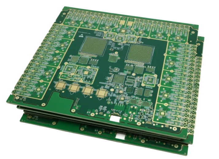
In the modern electronics landscape, "standard" fabrication parameters—like 8mil traces and simple through-holes—are no longer sufficient for high-performance applications. Advanced PCB manufacturing refers to the fabrication of printed circuit boards that utilize high-density interconnect (HDI) technologies, exotic materials, sequential lamination cycles, and extreme precision tolerances to achieve miniaturization and signal integrity that standard boards cannot match.
For engineers and product designers, moving into the realm of advanced manufacturing means navigating a complex set of Design for Manufacturing (DFM) constraints. It requires a shift from thinking about "connections" to thinking about transmission lines, thermal management, and material physics. Whether you are designing for aerospace avionics, 5G infrastructure, or medical devices, understanding the capabilities of your fabrication partner is the difference between a successful NPI and a costly yield disaster.
Quick Answer
Advanced PCB manufacturing involves processes beyond standard IPC Class 2 capabilities, typically including laser microvias, blind/buried vias, and trace widths below 3 mil (0.075mm).
- Critical Rule: Maintain a microvia aspect ratio of 0.8:1 or less (depth to diameter) to ensure reliable plating.
- Common Pitfall: Ignoring copper balance on inner layers, leading to bow and twist during the multiple lamination cycles required for advanced boards.
- Verification Method: Use Interconnect Stress Testing (IST) or cross-section analysis to verify the integrity of stacked microvias and internal layer registration.
- Material Requirement: High-speed designs often require Low-Loss Laminates (e.g., Rogers, Megtron) mixed with standard FR4 (Hybrid Stackup).
- Key Tech: Backdrilling is essential for signals >10Gbps to remove via stubs that cause signal reflection.
Highlights
- Sequential Lamination: How building a board "layer by layer" enables blind and buried vias but impacts cost and lead time.
- Via-in-Pad Plated Over (VIPPO): The gold standard for BGA fanout in high-density designs, requiring precise planarization.
- Hybrid Stackups: Combining different materials (e.g., RF materials + FR4) to balance cost and signal performance.
- Registration Accuracy: Advanced equipment (LDI) is required to maintain layer-to-layer alignment within +/- 3mil on complex multilayers.
Advanced PCB Manufacturing: Definition and Scope
While "standard" PCB manufacturing follows a linear process (drill, plate, etch, laminate), advanced PCB manufacturing is iterative and non-linear. It encompasses technologies designed to overcome the physical space limitations of traditional boards. This includes HDI PCB (High Density Interconnect) structures, rigid-flex combinations, and heavy copper applications for power distribution.
The scope of advanced manufacturing is defined by the equipment and process controls required. For instance, standard mechanical drills cannot reliably create holes smaller than 0.15mm (6mil). Advanced manufacturing utilizes UV or CO2 lasers to ablate dielectric material, creating microvias as small as 0.075mm (3mil). Furthermore, the imaging process shifts from traditional film artwork to Laser Direct Imaging (LDI), which compensates for material movement during fabrication to ensure precise alignment of these microscopic features.
The decision to move to advanced manufacturing is usually driven by component package sizes (such as 0.4mm pitch BGAs) or signal integrity requirements. However, every "advanced" feature adds a lever that impacts yield and cost.
Tech / Decision Lever → Practical Impact
| Decision Lever / Spec | Practical Impact (Yield/Cost/Reliability) |
|---|---|
| Laser Microvias (Blind) | Increases routing density significantly; allows for via-in-pad. Cost Impact: High (requires laser time and extra plating cycles). |
| Sequential Lamination (2+N+2) | Enables connections between specific internal layers without drilling through the whole board. Risk: Increases thermal stress and registration challenges. |
| Backdrilling (Controlled Depth) | Removes unused via stubs to improve signal integrity for high-speed data. Constraint: Requires specific "keep-out" zones around the via for the larger drill bit. |
| Resin Plugging & Capping (VIPPO) | Provides a flat surface for soldering directly over vias. Reliability: Critical for fine-pitch BGAs but prone to "dimpling" if not planarized correctly. |
Advanced PCB Manufacturing Rules and Specifications
To ensure a successful build, designers must adhere to stricter rules than standard PCBs. In advanced manufacturing, the margin for error is microscopic. The following table outlines key specifications that APTPCB recommends for high-yield production.
| Rule / Feature | Recommended Value | Why it matters | How to verify |
|---|---|---|---|
| Min Trace / Space | 3mil / 3mil (0.075mm) | Below this, etching consistency drops, leading to impedance variations or opens/shorts. | AOI (Automated Optical Inspection) after etching. |
| Microvia Aspect Ratio | ≤ 0.8:1 | Plating solution cannot circulate effectively in deep, narrow holes, leading to weak connections. | Cross-section analysis (microsectioning). |
| Layer-to-Layer Registration | +/- 3mil (75µm) | Misalignment causes breakout (drill hitting outside the pad), severing connections. | X-Ray Inspection post-lamination. |
| Solder Mask Dam | ≥ 3mil (0.075mm) | Prevents solder bridging between fine-pitch pads. If too small, the mask may peel off. | Visual Inspection / 3D measurement. |
| Plating Thickness (Wrap) | Class 3: ≥ 12µm wrap | Ensures the connection between the surface copper and the via barrel doesn't crack under thermal stress. | Microsectioning per IPC-6012 Class 3. |
When dealing with High Frequency PCB designs, material selection becomes a specification in itself. Mixing materials (e.g., Rogers 4350B with FR4) requires careful attention to the CTE (Coefficient of Thermal Expansion) z-axis expansion to prevent delamination during reflow.
Advanced PCB Manufacturing Implementation Steps
Executing an advanced PCB build is a choreographed sequence of chemical, mechanical, and optical processes. Unlike standard boards which might see the lamination press once, an advanced HDI board might go through the press 3 or 4 times.
Implementation Process
Step-by-step execution guide for advanced fabrication
CAM engineers simulate the stackup to verify impedance and balance copper distribution. We check for "acid traps" in fine traces and verify that annular rings meet Class 2/3 requirements based on the drill chart.
Core layers are laminated, then laser drilled to create microvias. A plasma desmear process follows to remove resin residue from the bottom of the via, ensuring a clean copper-to-copper connection.
Vertical Continuous Plating (VCP) is used for uniform copper deposition. Microvias are often filled with copper (via-filling) to allow for stacked vias, followed by planarization to flatten the surface.
The processed sub-assemblies are aligned with prepreg and outer foils and pressed again. This cycle repeats for every layer of buried vias (e.g., a 3+N+3 build goes through lamination 4 times).
Advanced PCB Manufacturing Troubleshooting
Even with perfect design files, issues can arise during the complex manufacturing steps. Here are common failure modes in advanced PCBs and how we address them.
1. Microvia Separation (Post-Separation)
This is a critical failure where the plated copper separates from the target pad at the bottom of the microvia, usually detected after thermal stress (reflow).
- Cause: Insufficient desmear (resin residue left in the hole) or weak electroless copper bonding.
- Fix: Optimize plasma cleaning cycles and use high-reliability copper plating baths. Designers should avoid "stacked" microvias across more than 2 layers if possible; staggered microvias are mechanically more robust.
2. Registration Drift
As layers are added and pressed, materials stretch and shrink. In a 20-layer board, the inner layers might shift enough that a drill misses its pad.
- Cause: Material movement during lamination; poor scaling factors in CAM.
- Fix: We use X-Ray drilling to locate targets on inner layers and optimize the drill program dynamically. Designers must ensure adequate annular rings (minimum 4-5mil over drill size) to accommodate this tolerance.
3. Impedance Mismatch
High-speed signals reflect if the trace width or dielectric thickness varies.
- Cause: Over-etching of fine traces or variation in prepreg thickness after pressing.
- Fix: Use "dummy copper" (thieving) in open areas to equalize plating current density. Designers should consult our Impedance Calculator and specify controlled dielectric materials.

6 Essential Rules for Advanced PCB Manufacturing (Cheat Sheet)
| Rule / Guideline | Why It Matters (Physics/Cost) | Target Value / Action |
|---|---|---|
| Microvia Aspect Ratio | Ensures plating solution reaches the bottom for a solid connection. | Max 0.8:1 (e.g., 4mil hole, 3mil dielectric) |
| BGA Fanout Strategy | Determines layer count and manufacturing complexity. | Use Dog-bone for >0.5mm pitch; VIPPO for <0.5mm. |
| Copper Balance | Prevents warping (bow/twist) during high-temp lamination. | Symmetrical stackup relative to center. |
| Trace Width Tolerance | Critical for controlled impedance (50Ω/100Ω). | Specify +/- 10% (standard) or +/- 5% (advanced). |
| Material Selection | High-speed signals degrade on standard FR4 (loss tangent). | Use Low Dk/Df materials for >5GHz. |
| Backdrill Keep-out | Prevents the large backdrill bit from cutting adjacent traces. | 10-12mil clearance around the via. |
FAQ
Q: How much does advanced manufacturing increase the cost compared to standard PCBs?
A: It varies, but adding HDI layers (laser drilling + sequential lamination) typically increases the bare board cost by 30-50% per lamination cycle due to the extra processing time and yield risk. However, it often reduces the total layer count, which can offset some costs.
Q: What is the standard lead time for advanced PCBs?
A: While standard prototypes can be done in 24-48 hours, advanced boards (HDI, Rigid-Flex) usually require 8-15 working days depending on the number of lamination cycles. Check our Quick Turn PCB services for expedited options.
Q: Can I use standard FR4 for advanced HDI boards?
A: Yes, standard High-Tg FR4 is commonly used for HDI. However, for high-speed applications, we recommend specialized materials like Isola or Megtron. Visit our PCB Materials page for data sheets.
Q: What is the smallest BGA pitch you can support?
A: We routinely support 0.4mm pitch BGAs using VIPPO technology. For 0.35mm pitch or smaller, please consult our engineering team for a DFM review as it requires extremely tight registration tolerances.
Request a Quote / DFM Review for Advanced PCB Manufacturing
Ready to move your high-performance design into production? Ensure your data package is complete to avoid engineering delays.
- Gerber Files (RS-274X): Include all copper layers, solder mask, silkscreen, and drill files.
- IPC Netlist: Critical for verifying that the graphic data matches the logical connections.
- Fabrication Drawing: Specify Class 2 or Class 3, material requirements (Tg, Dk), and stackup details.
- Stackup Definition: If you have specific impedance requirements, define the dielectric thickness or ask us to propose a valid stackup.
- Drill Chart: Clearly distinguish between plated through-holes (PTH), non-plated holes (NPTH), and laser microvias.
Conclusion
Advanced PCB manufacturing is not just about making things smaller; it's about making them smarter and more reliable. By leveraging technologies like laser microvias, sequential lamination, and specialized materials, you can achieve performance levels that were impossible a decade ago. However, these capabilities come with strict physical rules. Success lies in the details—balancing your copper, managing aspect ratios, and collaborating with your manufacturer early in the design phase.
At APTPCB, we specialize in bridging the gap between complex designs and high-yield manufacturing. Whether you are building a prototype or scaling for mass production, our engineering team is here to guide your stackup and DFM strategy.
Signed, The Engineering Team at APTPCB