Definition, scope, and who this guide is for
The term AI-Native PCB refers to the high-performance printed circuit boards specifically engineered to support Artificial Intelligence hardware ecosystems, including training servers, inference accelerators, and edge computing nodes. Unlike standard electronics, these boards must handle massive data throughput, extreme thermal loads, and ultra-low signal latency simultaneously. As AI infrastructure converges with telecommunications, the requirements for these boards often overlap with high-frequency infrastructure like 5G AAU PCB (Active Antenna Unit) and 5G ADC PCB (Analog-to-Digital Converter) modules, creating a complex manufacturing challenge that demands precision beyond IPC Class 2 standards.
This playbook is designed for hardware engineers, NPI managers, and procurement leads who are transitioning from standard digital electronics to high-performance computing (HPC) hardware. It cuts through the marketing noise to focus on the physical realities of manufacturing: material selection, stackup integrity, and the specific validation steps required to prevent field failures in expensive AI clusters.
At APTPCB (APTPCB PCB Factory), we have observed that the primary cause of project delays in this sector is not design capability, but a misalignment between design intent and manufacturing reality. This guide serves as a decision-making framework to bridge that gap, ensuring your specifications translate into reliable hardware.
When to use AI-Native PCB (and when a standard approach is better)
Understanding the scope defined above allows us to determine exactly when the cost and complexity of an AI-Native PCB are justified versus when a standard high-speed design suffices.
Use an AI-Native approach when:
- Signal Speeds exceed 56Gbps PAM4: Standard FR4 cannot support the signal integrity required for modern AI interconnects without massive attenuation.
- Layer Counts exceed 18 layers: AI accelerators often require high-density routing and extensive power planes that standard lamination presses cannot align accurately without specialized tooling.
- Thermal Density is critical: If your GPU or TPU generates heat requiring liquid cooling or immersion cooling compatibility, standard soldermask and substrate materials may degrade.
- Integration with 5G Infrastructure: Designs incorporating 5G AAU PCB technology for edge AI require mixed-signal capabilities (RF + Digital) that demand hybrid stackups.
Stick to Standard High-Speed PCB when:
- IoT Edge Devices: Simple inference on microcontrollers (e.g., voice recognition) rarely needs exotic materials; standard FR4 with controlled impedance is usually sufficient.
- Legacy Interfaces: If the board primarily handles PCIe Gen 3 or lower, the cost premium for AI-grade ultra-low loss materials is unnecessary.
- Prototyping Logic Only: If you are validating logic at low speeds before scaling to full speed, standard materials can save significant cost during early revisions.
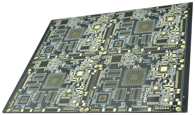
AI-Native PCB specifications (materials, stackup, tolerances)
Once you have determined that your project requires an AI-Native PCB, the next step is defining the rigid specifications that will govern the manufacturing process.
- Base Materials (Laminates):
- Requirement: Ultra-Low Loss materials are non-negotiable.
- Target: Df (Dissipation Factor) < 0.002 @ 10GHz; Dk (Dielectric Constant) < 3.6.
- Examples: Panasonic Megtron 7/8, Isola Tachyon 100G, or Rogers RO3000 series for hybrid RF sections.
- Copper Foil Roughness:
- Requirement: HVLP (Hyper Very Low Profile) or HVLP2 copper.
- Target: Surface roughness (Rz) < 1.5µm to minimize skin effect losses at high frequencies.
- Layer Count & Stackup:
- Range: Typically 20 to 40+ layers for server-grade boards.
- Structure: Multiple lamination cycles (3+); often requires "any-layer" HDI (High Density Interconnect) or ELIC (Every Layer Interconnect).
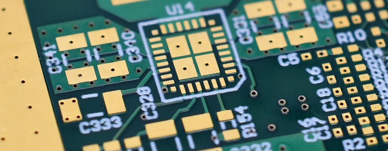
- Drilling & Vias:
- Backdrilling: Mandatory for high-speed signal layers to remove via stubs.
- Tolerance: Backdrill depth tolerance must be controlled within ±0.05mm to ±0.10mm to preserve signal integrity without cutting internal layers.
- Aspect Ratio: High aspect ratio plating capability (15:1 to 20:1) is required for thick boards (3.0mm+).
- Impedance Control:
- Tolerance: Tight control of ±5% or ±7% (standard is ±10%) on single-ended and differential pairs.
- Testing: 100% TDR (Time Domain Reflectometry) testing on coupons and production boards.
- Surface Finish:
- Preferred: ENIG (Electroless Nickel Immersion Gold) or ENEPIG for wire bonding support.
- Alternative: Immersion Silver for lower insertion loss, though shelf life is shorter.
- Thermal Reliability:
- Tg (Glass Transition Temp): > 180°C (High Tg).
- Td (Decomposition Temp): > 350°C to withstand multiple reflow cycles during assembly of large BGA components.
- Registration Accuracy:
- Target: Layer-to-layer registration within ±2-3 mils (50-75µm) to ensure pads align with vias in high-layer stacks.
- Cleanliness:
- Ionic Contamination: < 0.65µg/cm² NaCl equivalent, critical for preventing electrochemical migration in high-voltage data center environments.
AI-Native PCB manufacturing risks (root causes and prevention)
With specifications locked in, the focus shifts to mitigating the specific failure modes associated with manufacturing high-performance AI-Native PCB designs.
- Conductive Anodic Filament (CAF) Growth
- Root Cause: High voltage bias between closely spaced vias combined with moisture absorption in the resin system.
- Detection: CAF testing (1000+ hours at high temp/humidity).
- Prevention: Use CAF-resistant materials (spread glass weave) and maximize via-to-via spacing where possible.
- Pad Cratering
- Root Cause: Brittle laminate materials (common in high-speed materials) fracture under the mechanical stress of large BGA thermal expansion.
- Detection: Acoustic microscopy or dye-and-pry testing during validation.
- Prevention: Use resin-strengthened laminates and corner bonding/underfill on large BGAs.
- Signal Integrity Loss due to Etch Variation
- Root Cause: Over-etching or under-etching of trapezoidal traces changes the impedance profile.
- Detection: Cross-section analysis and TDR testing.
- Prevention: Specify "etch compensation" factors in CAM engineering and use vacuum etching equipment.
- Delamination during Reflow
- Root Cause: Trapped moisture in thick boards vaporizes during lead-free reflow temperatures (260°C).
- Detection: SAM (Scanning Acoustic Microscopy) after reflow simulation.
- Prevention: Strict baking protocols (4-8 hours) before assembly and moisture barrier packaging (MBB).
- Backdrill Stub Residue
- Root Cause: Drill bit wear or depth miscalculation leaves a small conductive stub.
- Detection: X-ray inspection or specific TDR analysis looking for reflection anomalies.
- Prevention: Automated optical drill bit checks and X-ray verification of the first article.
- Warpage / Bow and Twist
- Root Cause: Asymmetric copper distribution or unbalanced stackup in large format boards.
- Detection: Shadow Moiré measurement.
- Prevention: strictly balanced copper pouring on all layers; use of low-CTE materials.
- Plating Voids in High Aspect Ratio Vias
- Root Cause: Plating solution fails to circulate effectively in deep, narrow holes (e.g., 3mm thick board with 0.2mm vias).
- Detection: Cross-sectioning and thermal shock testing.
- Prevention: Pulse plating technology and aspect ratio design limits (keep below 15:1 if possible).
- Impedance Discontinuity at Layer Transitions
- Root Cause: Misalignment between the via pad and the reference plane clearance.
- Detection: VNA (Vector Network Analyzer) testing.
- Prevention: Laser direct imaging (LDI) for inner layers to ensure precise alignment.
AI-Native PCB validation and acceptance (tests and pass criteria)

To ensure the risks above are managed, a robust validation plan must be executed before mass production of any AI-Native PCB.
- Interconnect Stress Test (IST):
- Objective: Verify via reliability under thermal cycling.
- Method: Cycle coupons from ambient to 150°C (or higher) repeatedly.
- Acceptance: No resistance increase > 10% after 500 cycles.
- Signal Integrity (S-Parameter) Verification:
- Objective: Confirm insertion loss and return loss meet simulation models.
- Method: VNA measurement up to 28GHz or 56GHz.
- Acceptance: Insertion loss deviation < 1dB/inch from simulation; Return loss < -15dB.
- Hipot (High Potential) Testing:
- Objective: Ensure isolation between high-voltage power rails (common in AI server power delivery).
- Method: Apply high voltage (e.g., 500V-1000V) between nets.
- Acceptance: Leakage current < 1mA; no breakdown.
- Thermal Shock Testing:
- Objective: Test material bond strength and via plating integrity.
- Method: -55°C to +125°C liquid-to-liquid transfer.
- Acceptance: No delamination, blistering, or open circuits after 100 cycles.
- Solderability Test:
- Objective: Ensure surface finish accepts solder properly.
- Method: IPC J-STD-003 (Dip and Look or Wetting Balance).
- Acceptance: > 95% coverage; wetting time < 2 seconds.
- Ionic Contamination Test (ROSE):
- Objective: Verify board cleanliness.
- Method: IPC-TM-650 2.3.25.
- Acceptance: < 1.56 µg/cm² NaCl equivalent (often stricter for AI: < 0.65).
- Copper Peel Strength:
- Objective: Verify adhesion of copper to the dielectric.
- Method: Mechanical peel test.
- Acceptance: > 0.8 N/mm (or per material datasheet spec).
- Dimensional Stability:
- Objective: Ensure the board fits the chassis and aligns with sockets.
- Method: CMM (Coordinate Measuring Machine).
- Acceptance: Tolerances within ±0.1mm for outline; Warpage < 0.75%.
AI-Native PCB supplier qualification checklist (RFQ, audit, traceability)
When selecting a partner like APTPCB, use this checklist to ensure the factory is truly capable of handling AI-Native PCB requirements rather than just standard production.
Group 1: RFQ Inputs (What you must provide)
- Complete Gerber X2 or ODB++ files (preferred for complex data).
- IPC-356 Netlist for electrical test verification.
- Detailed Stackup Drawing specifying material types (brand/series) and dielectric thickness.
- Impedance Table referencing specific layers and trace widths.
- Drill Drawing distinguishing between through-holes, blind/buried vias, and backdrills.
- Fabrication Drawing with notes on Class 3 requirements (if applicable).
- Panelization requirements (if assembly requires specific rails/fiducials).
- Readme file highlighting critical nets (e.g., "Do not modify routing on Net X").
Group 2: Capability Proof (What the supplier must show)
- Equipment List: Laser Direct Imaging (LDI) machines for inner layers.
- Equipment List: Vacuum Etching lines (for fine lines < 3 mil).
- Equipment List: Automated Backdrilling machines with depth control sensing.
- Experience: Case studies or blinded samples of 20+ layer boards.
- Material Stock: Proof of inventory or direct supply chain for Megtron/Rogers materials.
- HDI Capability: Demonstrated ability for stacked microvias (e.g., 3+N+3).
Group 3: Quality System & Traceability
- Certifications: ISO 9001 (General), IATF 16949 (if automotive AI), UL 94V-0.
- Traceability: Can they trace a specific board to the raw material batch and lamination press cycle?
- IQC (Incoming Quality Control): Procedure for verifying pre-preg and core material properties.
- AOI (Automated Optical Inspection): Is AOI performed on every inner layer?
- Cross-Sectioning: Frequency of micro-section analysis per production lot.
Group 4: Change Control & Delivery
- PCN (Product Change Notification) Policy: Commitment to notify before changing materials or sub-suppliers.
- EQ (Engineering Question) Process: How they handle DFM discrepancies (formal report vs. email).
- Packaging: Moisture Barrier Bags (MBB) with HIC (Humidity Indicator Cards) and desiccant.
- Logistics: Experience shipping heavy copper/heavy weight shipments internationally.
How to choose AI-Native PCB (trade-offs and decision rules)
Every engineering decision involves a trade-off. Here is how to navigate the most common conflicts when specifying AI-Native PCB architectures.
- Material Cost vs. Signal Integrity
- Rule: If your total trace length is short (< 5 inches) and speed is < 25Gbps, you may use "Mid-Loss" material (e.g., Isola FR408HR).
- Rule: If trace length is long or speed > 25Gbps, you must choose "Ultra-Low Loss" (e.g., Megtron 7). The signal attenuation cost of FR4 will require expensive re-spins.
- HDI vs. Through-Hole
- Rule: If you have BGA components with pitch < 0.65mm, you must use HDI (Microvias).
- Rule: If BGA pitch is > 0.8mm, stick to Through-Hole or simple blind vias to reduce board cost by 30-50%.
- Backdrilling vs. Blind Vias
- Rule: If you need to remove stubs on a thick board (3mm+), Backdrilling is generally more cost-effective than sequential lamination (Blind Vias) for simple stub removal.
- Rule: If you need routing space on outer layers above the via, use Blind Vias.
- Surface Finish: ENIG vs. OSP
- Rule: If reliability and shelf life are paramount (Server/Data Center), choose ENIG.
- Rule: If signal integrity at extremely high frequency (> 50GHz) is the only priority, OSP (Organic Solderability Preservative) has no nickel layer to cause magnetic losses, but assembly must happen immediately.
- Board Thickness vs. Aspect Ratio
- Rule: If the board must be thick (for rigidity/layers), you must increase via diameter to maintain a plating aspect ratio < 15:1.
- Rule: If via size is fixed (small), you must reduce board thickness or accept higher yield loss/cost.
AI-Native PCB FAQ (cost, lead time, Design for Manufacturability (DFM) files, materials, testing)
Q: How does the cost of AI-Native PCB compare to standard PCBs? A: Expect costs to be 3x to 10x higher than standard FR4 boards. This is driven by expensive raw materials (Megtron/Rogers can be 5x FR4 cost), low-yield processes (HDI, backdrilling), and extensive testing requirements.
Q: What is the typical lead time for AI-Native PCB prototypes? A: Standard lead time is 15-20 working days due to sequential lamination cycles.
- Expedited: Can be pushed to 10-12 days with premium fees.
- Material Delay: Always check stock for exotic materials; ordering materials can add 2-4 weeks if not in stock.
Q: What specific DFM files are needed for AI-Native PCB impedance modeling? A: You must provide a stackup file that explicitly states the dielectric constant (Dk) and dissipation factor (Df) at the operating frequency (e.g., 10GHz), not just the 1MHz value found in generic datasheets.
Q: Can we mix materials (Hybrid Stackup) to save cost? A: Yes, this is common in 5G AAU PCB designs.
- Method: Use expensive high-frequency material for signal layers and cheaper FR4 for power/ground/mechanical layers.
- Risk: CTE mismatch between materials can cause warpage; requires careful engineering validation.
Q: What are the acceptance criteria for backdrilling depth? A: The industry standard is typically "Must not cut into the target layer copper" and "Remaining stub length < 10 mils (0.25mm)". Tighter tolerances (e.g., < 6 mils) increase cost and risk of open circuits.
Q: How do you test for reliability in 5G ADC PCB sections? A: Beyond standard E-test, we recommend specific noise floor testing and passive intermodulation (PIM) testing if the ADC is integrated with RF transmission lines.
Q: Why is "thieving" or copper balancing critical for these boards? A: AI boards are often large. Uneven copper distribution leads to "bow and twist" during reflow, which causes BGA solder joint failures. Automated copper thieving is added to empty areas to balance the stress.
Q: Do I need to specify IPC Class 3 for AI hardware? A: While IPC Class 2 is standard, most AI infrastructure owners specify "IPC Class 2 with Class 3 plating requirements" (i.e., thicker copper in vias) to ensure long-term reliability without the full cost/inspection burden of Class 3.
Resources for AI-Native PCB (related pages and tools)
- High-Speed PCB Manufacturing: Deep dive into the specific manufacturing techniques for signal integrity > 25Gbps.
- Server & Data Center PCB: Understand the specific reliability standards required for 24/7 operating environments.
- HDI PCB Capabilities: Learn about microvia structures and sequential lamination needed for high-density AI chips.
- Impedance Calculator: A tool to estimate trace width and spacing before submitting your final stackup.
- Panasonic Megtron PCB Materials: Specifications for the most common low-loss material used in AI accelerators.
- DFM Guidelines: Essential design rules to ensure your AI board is manufacturable at scale.
Request a quote for AI-Native PCB (Design for Manufacturability (DFM) review + pricing)
Ready to move from design to validation? At APTPCB, we provide a comprehensive DFM review alongside your quote to identify potential signal integrity or stackup risks before production begins.
To get an accurate quote and DFM, please prepare:
- Gerber/ODB++ Files: Complete data set.
- Stackup & Impedance: Desired layer count and target impedance.
- Material Spec: Specific laminate requirements (e.g., "Megtron 7 or equivalent").
- Volume: Prototype quantity vs. Mass production targets.
Click here to Request a Quote & DFM Review
Conclusion (next steps)
Successfully deploying an AI-Native PCB requires a shift in mindset from "connecting components" to "designing a transmission line system." By strictly defining your material specifications, understanding the risks of high-layer construction, and validating your supplier's capability to handle backdrilling and HDI, you can secure the hardware foundation your AI algorithms rely on. Whether you are building a 5G AAU PCB or a massive training cluster, the physics of manufacturing remain the ultimate gatekeeper to performance.