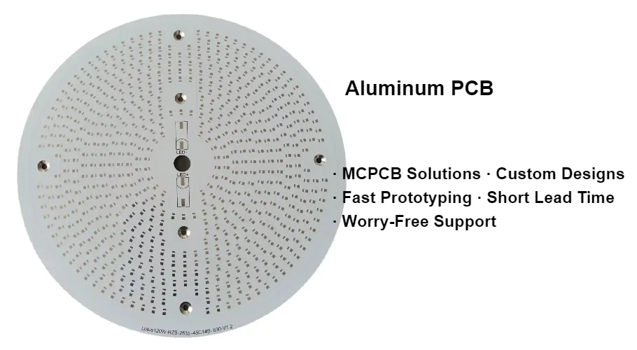
An aluminum PCB, often referred to as an Insulated Metal Substrate (IMS) or Metal Core PCB (MCPCB), is a printed circuit board that utilizes a base metal layer to dissipate heat significantly faster than standard FR4 materials. These boards are the industry standard for high-power applications—such as LED lighting and power converters—where efficient thermal management is the primary factor determining component reliability and lifespan.
Key Takeaways
- Thermal Conductivity is Critical: The dielectric layer typically ranges from 1.0 W/mK to 8.0 W/mK; selecting the correct value prevents component overheating.
- Dielectric Breakdown Voltage: Standard IMS dielectrics must withstand > 3.0 kV AC to ensure safety in high-voltage applications.
- Single-Layer Dominance: Over 90% of aluminum PCBs are single-sided due to the complexity and cost of insulating vias in multilayer metal stacks.
- Alloy Selection Matters: 5052 aluminum is preferred for general use due to its balance of strength and cost, while 6061 is chosen for complex machining.
- Solder Mask Reflectivity: For an aluminum led pcb, white solder mask with high reflectivity (> 85%) is essential for maximizing lumen output.
- Validation Tip: Always perform a Hi-Pot (High Potential) test at 1000V + 2×Vrated to verify the integrity of the dielectric layer before assembly.
- Decision Rule: If your component power density exceeds 0.5 W/cm², standard FR4 is likely insufficient, and an aluminum substrate is required.
Contents
- What It Really Means (Scope & Boundaries)
- Metrics That Matter (How to Evaluate It)
- How to Choose (Selection Guidance by Scenario)
- Implementation Checkpoints (Design to Manufacturing)
- Common Mistakes (and the Correct Approach)
- FAQ (Cost, Lead Time, Materials, Testing, Acceptance Criteria)
- Glossary (key terms)
- Conclusion (next steps)
What It Really Means (Scope & Boundaries)
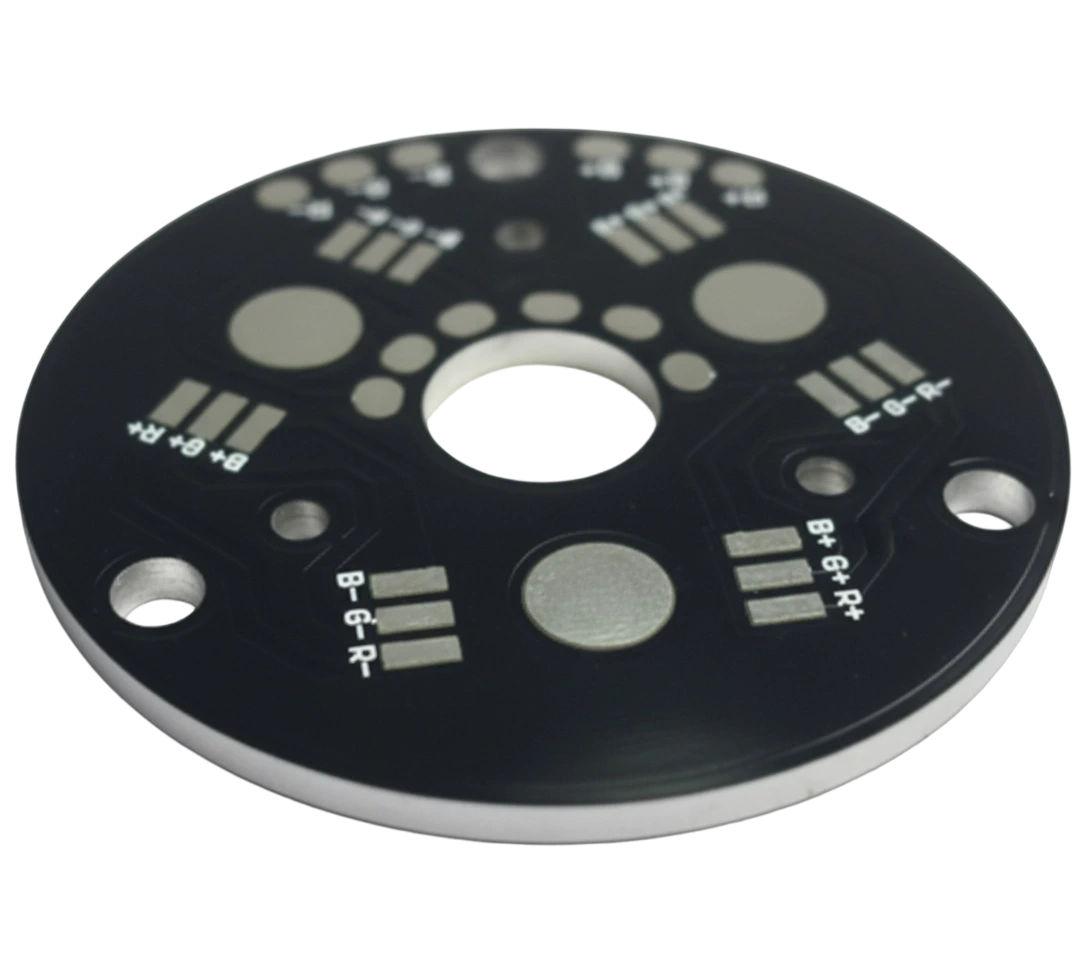
An aluminum PCB is defined by its unique stackup, which differs fundamentally from traditional rigid boards. While a standard PCB uses a fiberglass-epoxy substrate (FR4), an aluminum PCB uses a metal plate as the structural base. The core function of this stackup is to act as a thermal bridge, moving heat away from critical components (like LEDs or MOSFETs) to a heatsink or the chassis.
The structure consists of three distinct layers:
- Circuit Layer: Typically copper foil ranging from 1 oz (35µm) to 10 oz (350µm). This layer carries the electrical signal and current.
- Dielectric Layer: This is the most critical component. It is a thermally conductive but electrically insulating ceramic-filled polymer. Its thickness usually ranges from 50µm to 150µm. This layer determines the board's thermal performance (impedance) and electrical safety (breakdown voltage).
- Base Layer: The aluminum substrate, typically 1.0mm to 3.0mm thick. It provides mechanical rigidity and acts as the primary heat spreader.
Unlike FR4, which acts as a thermal insulator (conductivity ~0.25 W/mK), the dielectric in an aluminum PCB is engineered to conduct heat 5 to 30 times more efficiently. This capability allows engineers to push components to higher currents without requiring bulky active cooling systems.
Metrics That Matter (How to Evaluate It)
When specifying an aluminum PCB, you are primarily specifying the properties of the dielectric material and the aluminum alloy. The following tables outline the critical ranges and acceptance criteria for high-quality production.
Table 1: Thermal and Mechanical Properties
| Metric | Typical Range | Why It Matters | How to Verify |
|---|---|---|---|
| Thermal Conductivity | 1.0 – 8.0 W/mK | Determines how fast heat moves from the component to the aluminum base. Higher is better but more expensive. | ASTM D5470 test method on the dielectric material. |
| Thermal Resistance (Rth) | 0.05 – 0.45 °C/W | The opposition to heat flow. Lower values mean cooler junction temperatures for LEDs. | Calculated based on dielectric thickness and conductivity. |
| Glass Transition (Tg) | 100°C – 180°C | The temperature at which the dielectric softens. High Tg is needed for lead-free soldering. | TMA (Thermomechanical Analysis) or DSC methods. |
| Peel Strength | 1.0 – 1.8 N/mm | Measures how well the copper bonds to the dielectric. Prevents delamination during assembly. | IPC-TM-650 2.4.8 peel test. |
| CTE (Z-axis) | 20 – 50 ppm/°C | Coefficient of Thermal Expansion. Lower values reduce stress on solder joints during thermal cycling. | TMA measurement across temperature range. |
Table 2: Electrical and Alloy Specifications
| Metric | Typical Range | Why It Matters | How to Verify |
|---|---|---|---|
| Breakdown Voltage (AC) | 3.0 kV – 6.0 kV | The voltage at which the dielectric fails and arcs to the aluminum base. Critical for safety. | Hi-Pot testing per IPC-TM-650 2.5.6. |
| Volume Resistivity | 10⁶ – 10⁹ MΩ·cm | Ensures the dielectric is a true insulator and prevents leakage current. | High resistance meter measurement. |
| Aluminum Alloy | 1060, 5052, 6061 | 1060 is soft/cheap; 5052 is rigid/standard; 6061 is hard/machinable. | Material certification (Mill Test Report). |
| Copper Thickness | 35µm – 350µm | Thicker copper spreads heat laterally before it passes vertically through the dielectric. | Microsection analysis (cross-section). |
| Solder Mask Reflectivity | > 85% (White) | For aluminum led pcb applications, reflects light outward rather than absorbing it. | Reflectometer or spectrophotometer. |
How to Choose (Selection Guidance by Scenario)
Selecting the right specifications requires balancing thermal performance, electrical isolation, and cost. Use the following decision rules to guide your engineering choices.
- If the application is general LED lighting (< 1W per LED), choose a standard 1.0 W/mK dielectric with 1 oz copper. This is the most cost-effective volume solution.
- If you are designing high-power street lights or automotive headlights, choose a dielectric with 2.0 W/mK to 3.0 W/mK conductivity to manage the concentrated heat flux.
- If the operating voltage exceeds 400V (e.g., EV power trains), choose a high-voltage dielectric rated for > 5.0 kV breakdown and verify the CTI (Comparative Tracking Index) is Grade 0.
- If the board requires complex CNC machining or screw tapping, choose 6061 aluminum alloy because it is harder and machines cleaner than the softer 5052 or 1060 alloys.
- If the board will be bent or formed (rare but possible), choose 5052 alloy and a flexible dielectric specifically designed for bending radii > 10mm.
- If you need to maximize lateral heat spreading before vertical dissipation, choose 2 oz or 3 oz copper foil. This increases the heat transfer area into the dielectric.
- If you are unsure how to specify ims stackup for high power led arrays, choose a thinner dielectric (e.g., 75µm instead of 100µm) to reduce thermal resistance, provided it meets voltage requirements.
- If the environment involves high vibration (aerospace/automotive), choose a high peel strength material (> 1.4 N/mm) to ensure traces do not lift under mechanical stress.
- If cost is the absolute driver and thermal requirements are low, choose 1060 alloy, but be aware it is very soft and can deform during V-scoring.
- If the design requires plated through-holes (PTH), choose a different technology (like thick copper FR4 or copper pedestal) or a complex "hybrid" build, as standard aluminum PCBs are strictly single-sided.
Implementation Checkpoints (Design to Manufacturing)
Successfully moving an aluminum PCB from concept to production requires strict adherence to specific design and manufacturing protocols. Follow this 10-step checklist.
1. Stackup Definition
- Action: Define the specific conductivity and dielectric thickness in the fabrication notes.
- Acceptance Check: Fab notes explicitly state "Dielectric: 2.0 W/mK, 100µm thickness" rather than generic "MCPCB".
- Criteria: Manufacturer confirms material availability in stock (e.g., Bergquist, Laird, or equivalent Asian brands).
2. Circuit Design (Trace Width)
- Action: Widen high-current traces to account for the current carrying capacity.
- Acceptance Check: Verify trace widths against IPC-2152 standards, adjusting for the superior cooling of aluminum (which allows slightly higher current per width).
- Criteria: Temperature rise < 10°C at max current in simulation.
3. Electrical Isolation (Clearance)
- Action: Maintain sufficient clearance between copper features and the board edge (or V-score line).
- Acceptance Check: Minimum clearance from copper to V-cut center is > 0.5mm (preferably 1.0mm) to prevent arcing to the aluminum base.
- Criteria: No copper exposed on the cut edge after depanalization.
4. Solder Mask Selection
- Action: Select "Super White" or "LED White" solder mask for lighting applications.
- Acceptance Check: Verify the mask is non-yellowing (high reflectivity retention) after reflow.
- Criteria: Reflectivity > 85% and color change (Delta E) < 1.0 after 2x reflow cycles.
5. Panelization Strategy
- Action: Choose V-scoring (V-cut) for rectangular boards; use routing/punching for complex shapes.
- Acceptance Check: For V-cut, ensure the web thickness is sufficient (typically 1/3 of total thickness) to hold the panel together during assembly.
- Criteria: Panel remains rigid during pick-and-place but snaps cleanly without bending the aluminum.
6. Surface Finish Application
- Action: Select HASL (Hot Air Solder Leveling) or ENIG (Electroless Nickel Immersion Gold).
- Acceptance Check: HASL is cheaper but less flat; ENIG is flat and better for wire bonding.
- Criteria: Solder pad flatness variation < 5µm for ENIG (critical for fine-pitch LEDs).
7. Mechanical Drilling
- Action: Minimize the number of holes to reduce drill bit wear and cost.
- Acceptance Check: Ensure hole diameters are large enough (> 1.0mm preferred) to prevent drill breakage in the aluminum.
- Criteria: No burrs on the aluminum side; hole wall roughness < 30µm.
8. Hi-Pot Testing (Fabrication)
- Action: Perform 100% electrical isolation testing on bare boards.
- Acceptance Check: Apply high voltage between the circuit layer and the aluminum base.
- Criteria: No breakdown or leakage current > 1mA at 1000V DC (or specified voltage).
9. Assembly Reflow Profile
- Action: Adjust reflow oven profile to account for the high thermal mass of aluminum.
- Acceptance Check: Increase soak time and peak temperature duration compared to FR4.
- Criteria: Solder joints show good wetting (meniscus) and voiding < 25% under X-ray.
10. Final Quality Audit
- Action: Inspect for warping and surface defects.
- Acceptance Check: Aluminum PCBs can warp if the CTE mismatch is high.
- Criteria: Bow and twist < 0.75% (IPC Class 2 standard).
Common Mistakes (and the Correct Approach)
Errors in specifying aluminum PCBs often lead to electrical shorts or poor thermal performance.
1. Ignoring Dielectric Thickness vs. Voltage
- Mistake: Specifying a thin dielectric (e.g., 50µm) for high-voltage applications (> 500V) to improve thermals.
- Impact: High risk of dielectric breakdown and arcing to the chassis.
- Fix: Use a thicker dielectric (100µm–150µm) or a high-voltage specific material.
- Verify: Pass Hi-Pot test at 2000V+ without leakage.
2. Placing Vias for Interconnection
- Mistake: Designing a standard plated through-hole (PTH) to connect top and bottom layers.
- Impact: Short circuit to the aluminum core; standard manufacturing cannot insulate the hole wall from the core easily.
- Fix: Design as a single-layer board. If jumpers are needed, use 0Ω resistors.
- Verify: Gerber files show no plated holes (NPTH only).
3. Insufficient Copper-to-Edge Clearance
- Mistake: Routing copper traces too close (< 0.3mm) to the board edge or V-score.
- Impact: The V-scoring blade exposes the copper, or arcing occurs between the trace and the exposed aluminum edge.
- Fix: Maintain 0.5mm to 1.0mm clearance from copper to the cut line.
- Verify: DFM check specifically looking for copper-to-outline distance.
4. Using Standard FR4 Reflow Profiles
- Mistake: Using the same reflow profile as a standard fiberglass board.
- Impact: Cold solder joints because the aluminum base sucks heat away too fast for the solder to wet properly.
- Fix: Use a "hotter" profile with a longer soak zone to bring the aluminum mass up to temperature.
- Verify: Cross-section analysis of solder joints showing intermetallic compound formation.
5. Over-Specifying Thermal Conductivity
- Mistake: Requesting 5.0 W/mK material for a 0.5W LED application.
- Impact: Unnecessary cost increase (2x–3x material cost) with negligible performance benefit.
- Fix: Calculate the required Rth; usually, 1.0–2.0 W/mK is sufficient for low-to-mid power.
- Verify: Thermal simulation showing junction temperature is well within safe limits with standard material.
6. Wrong Alloy for Mechanical Processing
- Mistake: Using 1060 alloy for a design requiring tapped screw holes.
- Impact: Threads strip easily because 1060 is too soft.
- Fix: Specify 6061-T6 or 5052-H34 for designs involving threading or structural loads.
- Verify: Material certification and mechanical torque testing on threads.
7. Neglecting Thermal Expansion (Cte) Mismatch
- Mistake: Using large ceramic components on a board with high CTE mismatch.
- Impact: Solder joints crack after thermal cycling due to different expansion rates of the component vs. the board.
- Fix: Use dielectric with matched CTE or flexible termination components.
- Verify: Thermal shock testing (-40°C to +125°C) for 500+ cycles.
8. Assuming "Aluminum PCB" Means "Multilayer"
- Mistake: Designing a 4-layer board and assuming it can be easily made on an aluminum base.
- Impact: Extremely high cost and limited suppliers. Most "multilayer" aluminum boards are actually FR4 boards bonded to aluminum.
- Fix: Consult with the manufacturer early. Usually, it is better to use a Metal Core PCB hybrid approach or standard rigid board bonded to a heat spreader.
- Verify: Stackup confirmation before starting layout.
FAQ (Cost, Lead Time, Materials, Testing, Acceptance Criteria)
1. How does the cost of aluminum PCB compare to FR4? Aluminum PCBs are typically 20–50% more expensive than single-sided FR4 due to the raw material cost of the aluminum and the specialized dielectric. However, they eliminate the need for separate heatsinks and thermal grease, often lowering the total system cost for high-power assemblies.
- FR4: Low material cost, requires secondary heatsink assembly.
- Aluminum: Higher board cost, reduced assembly labor and BOM count.
2. What is the standard lead time for manufacturing? Standard lead times are slightly longer than FR4 due to material availability and mechanical processing (punching/V-scoring).
- Prototype: 3–5 days.
- Mass Production: 10–15 days.
- Expedited: 24–48 hours is possible for stock materials (1W/mK, 1.6mm).
3. Can I use plated through-holes (PTH) on an aluminum PCB? Generally, no. Standard aluminum PCBs are single-sided (1 layer).
- Reason: Drilling through aluminum and insulating the hole wall to plate copper is a complex, expensive process.
- Alternative: Use 0Ω jumpers for routing crossovers or explore Rigid-Flex PCB solutions if 3D routing is required.
4. What is the maximum voltage rating for these boards? The voltage rating depends entirely on the dielectric thickness and quality.
- Standard (100µm): Typically rated for 3kV AC breakdown.
- High-Voltage: Can go up to 5kV–8kV with specialized dielectrics.
- Verification: Always specify the required Hi-Pot test voltage in your fabrication notes.
5. How do I specify the stackup for a high-power LED application? To correctly address how to specify ims stackup for high power led designs, focus on thermal resistance.
- Base: 1.6mm Aluminum 5052 (standard stiffness).
- Dielectric: 2.0 W/mK or higher, 75µm–100µm thickness (thinner transfers heat faster but lowers breakdown voltage).
- Copper: 1 oz (35µm) minimum; use 2 oz (70µm) if current > 1A to help lateral spreading.
6. What surface finishes are available? The options are similar to standard PCBs, but HASL and OSP are most common.
- HASL (Lead-Free): Most common, robust, good shelf life.
- OSP: Flat, cheap, but sensitive to handling.
- ENIG: Best for wire bonding or very flat pads, but more expensive.
7. Can aluminum PCBs be reworked? Rework is difficult due to the high thermal conductivity.
- Challenge: The aluminum base sinks the heat from the soldering iron instantly.
- Solution: You must use a pre-heater (hot plate) set to 100°C–120°C to raise the base temperature before attempting to desolder/solder components.
8. What testing is performed during manufacturing? Beyond standard visual and dimensional checks, specific tests for
Glossary (Key Terms)
| Term | Meaning | Why it matters in practice |
|---|---|---|
| DFM | Design for Manufacturability: layout rules that reduce defects. | Prevents rework, delays, and hidden cost. |
| AOI | Automated Optical Inspection used to find solder/assembly defects. | Improves coverage and catches early escapes. |
| ICT | In-Circuit Test that probes nets to verify opens/shorts/values. | Fast structural test for volume builds. |
| FCT | Functional Circuit Test that powers the board and checks behavior. | Validates real function under load. |
| Flying Probe | Fixtureless electrical test using moving probes on pads. | Good for prototypes and low/medium volume. |
| Netlist | Connectivity definition used to compare design vs manufactured PCB. | Catches opens/shorts before assembly. |
| Stackup | Layer build with cores/prepreg, copper weights, and thickness. | Drives impedance, warpage, and reliability. |
| Impedance | Controlled trace behavior for high-speed/RF signals (e.g., 50Ω). | Avoids reflections and signal integrity failures. |
| ENIG | Electroless Nickel Immersion Gold surface finish. | Balances solderability and flatness; watch nickel thickness. |
| OSP | Organic Solderability Preservative surface finish. | Low cost; sensitive to handling and multiple reflows. |
Conclusion
aluminum pcb is easiest to get right when you define the specifications and verification plan early, then confirm them through DFM and test coverage.
Use the rules, checkpoints, and troubleshooting patterns above to reduce iteration loops and protect yield as volumes increase.
If you’re unsure about a constraint, validate it with a small pilot build before locking the production release.