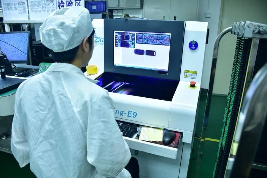
Automated Optical Inspection (AOI) is the primary non-contact method for verifying printed circuit board assembly (PCBA) quality by comparing captured images against defined parameters or a "golden board." It serves as a critical gatekeeper in Surface Mount Technology (SMT) lines, detecting defects like component skew, missing parts, and solder bridging before boards move to functional testing. Mastering aoi basics ensures manufacturers catch 90% or more of visible defects early, reducing rework costs and preventing field failures.
Quick Answer (30 Seconds)
- Core Rule: Component displacement must not exceed 50% of the pad width for IPC Class 2, or 25% for IPC Class 3.
- Critical Range: Camera resolution should be set between 10 µm and 15 µm per pixel to reliably inspect 0201 or 01005 components.
- Common Pitfall: Relying solely on 2D AOI for BGA inspection; 2D cannot see hidden solder joints beneath the package body.
- Verification: Use a known defect board (verification artifact) with at least 10 types of simulated errors (e.g., tombstone, short, missing) to validate machine detection daily.
- Boundary Case: Highly reflective components (like certain LEDs or metal cans) often trigger false calls due to lighting glare; use polarized lighting or 3D AOI to compensate.
- DFM Tip: Ensure component footprints in the CAD data match the physical parts exactly; a 0.5mm mismatch in the library definition causes persistent false rejects.
Highlights
- Defect Coverage: Detects visible surface defects including polarity, skew, wetting, and text (OCR).
- Speed vs. Accuracy: Typical inspection speeds range from 20 to 40 cm²/sec depending on resolution settings.
- False Call Rate: A well-tuned AOI process targets a false call rate below 500 PPM (parts per million).
- Lighting Importance: Multi-angle LED lighting (Red/Green/Blue) is essential for distinguishing between copper, solder, and silk screen.
- 3D Capability: 3D AOI measures height (Z-axis), critical for detecting lifted leads and coplanarity issues > 150 µm.
- Integration: AOI data often feeds into statistical process control (SPC) to trend defect rates in real-time.
Contents
- Definition and Scope (What It Is, What It Isn’t)
- Rules and Specifications (Key Parameters and Limits)
- Implementation Steps (Process Checkpoints)
- Troubleshooting (Failure Modes and Fixes)
- How to Choose (Design Decisions and Trade-Offs)
- FAQ (Cost, Lead Time, Materials, Testing, Acceptance Criteria)
- Glossary (Key Terms)
- Request a Quote (DFM Review + Pricing)
- Conclusion (next steps)
Definition and Scope (What It Is, What It Isn’t)
Understanding aoi basics requires defining exactly where this technology fits in the manufacturing line. It is an optical inspection method, meaning it relies on line-of-sight.
Applies when:
- SMT Assembly: Verifying placement and soldering of chip resistors, capacitors, ICs, and connectors.
- Post-Reflow Inspection: Checking final solder joint criteria after the oven to ensure wetting and fillet formation.
- Pre-Reflow Inspection: Checking paste placement and component positioning before soldering to prevent hard-to-fix defects.
- Wave Soldering: Inspecting the bottom side of the PCB for through-hole solder joint quality (shorts, skips).
- 2D and 3D Inspection: Validating X, Y, and Z (height) dimensions of components and solder fillets.
Doesn’t apply when:
- Hidden Joints: It cannot inspect solder joints underneath Ball Grid Arrays (BGAs) or QFN thermal pads (requires X-Ray Inspection).
- Electrical Function: It does not verify if the component works electrically or if the firmware is loaded (requires ICT or FCT).
- Internal Layers: It cannot detect inner layer shorts or opens within the PCB laminate (requires E-Test during fabrication).
- Potting/Coating: Once a board is conformal coated or potted, AOI effectiveness drops significantly due to reflections and obscuration.
Rules and Specifications (Key Parameters and Limits)
The following table outlines the critical parameters for setting up and evaluating AOI performance. Adhering to these limits ensures the inspection process is robust and minimizes escapes (defects leaving the factory).
| Rule | Recommended Value/Range | Why It Matters | How to Verify | If Ignored |
|---|---|---|---|---|
| Component Shift (X/Y) | < 50% of pad width (Class 2) < 25% of pad width (Class 3) |
Ensures sufficient electrical contact and mechanical stability. | Measure distance from pad center to component center in AOI debug mode. | Risk of open circuits or weak joints that fail under vibration. |
| Component Rotation (Skew) | < 10 degrees (Chip components) < 2 degrees (Fine pitch ICs) |
Excessive rotation reduces solder contact area and risks bridging. | Check angle delta in AOI algorithm settings against CAD coordinates. | High risk of bridging on adjacent pads for fine-pitch ICs. |
| Solder Fillet Height | 25% to 100% of component termination height | Indicates proper wetting and solder volume. | Use 3D AOI height measurement or side-angle camera views. | Insufficient solder leads to joint cracking; excess solder causes rigidity issues. |
| Coplanarity (Lifted Lead) | < 100 µm (0.10 mm) deviation | Ensures all leads contact the solder paste during reflow. | 3D AOI laser triangulation or Moiré fringe projection. | Open circuits on specific pins of an IC (e.g., QFP, SOP). |
| Bridge/Short Detection | 0 µm gap (Continuity between distinct nets) | Solder bridging causes immediate electrical failure. | Algorithm checks for solder presence in the gap between pads. | Dead board; potential component damage upon power-up. |
| Missing Component | 100% presence check | Fundamental assembly requirement. | Pattern matching or histogram analysis of the component body. | Board fails function completely; costly troubleshooting later. |
| Polarity Check | Match silkscreen/fiducial mark | Critical for diodes, capacitors, and ICs to prevent reverse voltage damage. | OCR (Optical Character Recognition) or feature matching on body markings. | Component explosion or circuit malfunction. |
| Tombstoning | 0% tolerance (Vertical lift) | Component stands on one end, breaking the circuit. | Height check + absence of component body in the horizontal plane. | Open circuit; requires manual rework. |
| Solder Ball Detection | > 0.15 mm diameter (typically flagged) | Loose solder balls can dislodge and cause shorts elsewhere. | Blob analysis algorithms in non-pad areas. | Reliability risk; shorts occurring during shipping or operation. |
| False Call Rate | < 500 - 1000 PPM | High false calls slow down the line and desensitize operators. | Review logs of "False Fail" vs. "True Fail" over a shift. | Operators may start auto-passing boards, letting real defects escape. |
Implementation Steps (Process Checkpoints)
Implementing a robust AOI inspection process involves more than just turning on the machine. Follow these steps to integrate AOI effectively into the SMT assembly line.
Data Preparation and Import
- Action: Import Pick and Place (XY) data and Gerber files into the AOI software.
- Key Parameters: Ensure unit of measure matches (mm vs. mils) and rotation reference (0/90/180/270) is consistent with the machine library.
- Acceptance Check: Verify that all component locations on the virtual map align with the physical board pads.
Golden Board Creation
- Action: Scan a known "good" board to teach the machine the visual characteristics of acceptable joints and components.
- Key Parameters: Use a board with standard solder volume; avoid boards with hand-soldered touch-ups for the master sample.
- Acceptance Check: The machine should pass this board 100% of the time without false calls.
Algorithm Tuning and Library Matching
- Action: Assign inspection algorithms (e.g., lead inspection, body check, color match) to each component package type.
- Key Parameters: Set tolerance windows for brightness (0-255 scale) and position (+/- 0.1mm to 0.3mm).
- Acceptance Check: Verify that the algorithm correctly identifies the component body and the solder meniscus.
Lighting Optimization
- Action: Configure multi-angle lighting (Main, Side, Coaxial) to highlight specific features.
- Key Parameters: High-angle light for flat surfaces (markings); Low-angle light for 3D features (solder fillets, lifted leads).
- Acceptance Check: Solder joints should appear distinct from the PCB pad; text on chips should be legible.
Threshold Setting (Sensitivity)
- Action: Adjust the pass/fail thresholds to balance defect detection against false calls.
- Key Parameters: Set minimum solder area coverage (e.g., >75% of pad) and maximum shift tolerance.
- Acceptance Check: Run a "limit sample" (board with known marginal defects) to ensure the machine flags them.
Verification with Defect Board
- Action: Pass a test board with intentional defects (missing part, short, wrong polarity) through the machine.
- Key Parameters: The board should contain at least one of every major defect type relevant to the production run.
- Acceptance Check: Zero escapes allowed. The machine must catch 100% of the intentional defects.
Operator Training and SOP
- Action: Define how operators handle a "Fail" signal.
- Key Parameters: Review station setup; magnification tools (microscope) for manual verification.
- Acceptance Check: Operators must correctly classify "False Call" vs. "Real Defect" in the system log.
Continuous Feedback Loop
- Action: Link AOI data to the SMT printer and pick-and-place machines.
- Key Parameters: Trend analysis of offset values (e.g., consistent 50µm shift in X).
- Acceptance Check: If a trend is detected, the upstream machine (printer or mounter) is adjusted before defects occur.
Troubleshooting (Failure Modes and Fixes)
Even with high-end equipment, AOI processes can drift. Use this guide to diagnose common issues where aoi basics intersect with real-world variables.
1. Symptom: High False Call Rate on Solder Joints
- Likely Causes: Lighting reflection variation, oxidation on pads, or flux residue.
- Checks: Inspect the solder joint surface finish (HASL vs. ENIG reflect differently). Check lighting angle settings.
- Fix: Adjust the "solder brightness" threshold or switch to a different lighting color channel (e.g., use red light for better contrast on copper).
- Prevention: Standardize PCB surface finishes and paste formulations.
2. Symptom: Escaped "Missing Components"
- Likely Causes: Component color matches the PCB mask color (e.g., black component on black PCB).
- Checks: Verify the contrast difference between the part body and the background in the algorithm.
- Fix: Use 3D height inspection instead of 2D contrast. If 3D is unavailable, use side-lighting to cast a shadow.
- Prevention: Design rules should avoid color combinations that mask components, or mandate 3D AOI for such cases.
3. Symptom: False "Bridge" Calls on Fine Pitch ICs
- Likely Causes: Solder mask webbing is absent between pads; glare from flux looks like a bridge.
- Checks: Check if the PCB design has "solder mask defined" or "non-solder mask defined" pads. Look for shiny flux residues.
- Fix: Tune the "bridge detection window" to be narrower. Use polarized lighting to cut glare.
- Prevention: Ensure PCB fabrication includes solder mask dams between fine-pitch pads (min 3-4 mil width).
4. Symptom: Polarity Marks Not Detected
- Likely Causes: Markings are faint, laser-etched, or vary by batch/vendor.
- Checks: Compare the current component batch with the library image.
- Fix: Update the library with multiple "alternative" images for the same part. Enable "feature matching" (e.g., chamfered edge) instead of just text.
- Prevention: Specify consistent component vendors or require incoming inspection to flag marking changes.
5. Symptom: Tombstones Not Detected
- Likely Causes: The component is standing vertically but the top profile looks like a valid placement in 2D.
- Checks: Review the 2D image from the top-down camera.
- Fix: This is a classic 2D limitation. Enable 3D height check. If 2D only, look for the "shadow" of the standing component.
- Prevention: Use 3D AOI for 0402 components and smaller.
6. Symptom: Wrong Part Value Passed (e.g., 10k vs 100k Resistor)
- Likely Causes: Both parts are the same size and color; markings are too small or on the bottom.
- Checks: AOI cannot read electrical values. It can only read visible text.
- Fix: If text is visible, improve OCR resolution. If no text, AOI cannot fix this.
- Prevention: Implement electrical testing (ICT) or strict feeder verification (barcoding) during loading.
7. Symptom: Shadowing Effects on Tall Components
- Likely Causes: Tall capacitors blocking light to adjacent small resistors.
- Checks: Identify "blind spots" in the inspection map.
- Fix: Use an AOI system with multiple side cameras (4-way or 8-way projection).
- Prevention: DFM rule: Maintain minimum spacing between tall and short components (typically > 0.5mm or 1:1 height ratio).
How to Choose (Design Decisions and Trade-Offs)
Selecting the right inspection strategy depends on the complexity of the board and the reliability requirements.
If you have 0201 or 01005 components, choose 3D AOI. 2D systems struggle to distinguish the height of the solder fillet on microscopic parts. 3D volumetric measurement is essential for reliability here.
If you are assembling simple consumer electronics (Class 1), choose 2D AOI. For low-cost, low-complexity boards with large components (0603+), 2D inspection is faster and more cost-effective.
If you have high-mix, low-volume production, choose Offline AOI. Offline machines are easier to reprogram and don't stop the entire SMT line while debugging a new program.
If you have high-volume mass production, choose Inline AOI. Inline systems sit directly on the conveyor after the reflow oven, providing immediate feedback to the line to stop defects before thousands are made.
If you use BGA or QFN components, choose AOI + X-Ray (AXI). AOI cannot see beneath the package. You must supplement AOI with X-ray inspection to verify the hidden solder joints.
If you have tall connectors or shields, choose AOI with High Clearance. Ensure the machine's Z-axis clearance (typically 25mm - 50mm) exceeds your tallest component to prevent collision.
If you need to verify solder paste deposition, choose SPI (Solder Paste Inspection). Do not rely on post-reflow AOI to fix paste issues. Use SPI inspection before component placement to catch volume issues at the source.

FAQ (Cost, Lead Time, Materials, Testing, Acceptance Criteria)
1. What is the difference between AOI and SPI? SPI (Solder Paste Inspection) happens before component placement and measures paste volume. AOI happens after reflow (usually) and checks component placement and solder joint quality. Both are needed for a complete quality system.
2. Can AOI detect electrically defective components? No. AOI only checks visual characteristics (shape, position, markings, solder). It cannot tell if a chip is internally damaged or has the wrong firmware.
3. How long does it take to program an AOI machine for a new board? Typically 2 to 6 hours depending on complexity. Using CAD data (XY coordinates) speeds this up significantly compared to manual "teach" methods.
4. Does AOI replace manual visual inspection? Yes, for the most part. AOI is faster and more consistent than human eyes, which fatigue after 15 minutes. However, humans are still needed to verify the "fails" flagged by the AOI.
5. What is the typical false call rate target? A world-class process targets < 500 PPM. If the rate is higher, operators may ignore real defects. If it's 0, the sensitivity is likely too low, and escapes are occurring.
6. Can AOI inspect flexible PCBs? Yes, but the machine must handle the non-planar surface. Vacuum fixtures or specialized algorithms for flex PCB are often required to compensate for board warpage.
7. Is 3D AOI always better than 2D AOI? 3D is better for geometry (lifted leads, coplanarity, tombstoning) but is slower and more expensive. 2D is often better for reading text (OCR) and checking polarity markings.
8. What IPC standard governs AOI criteria? IPC-A-610 (Acceptability of Electronic Assemblies) is the standard used. AOI machines are programmed to detect defects defined in IPC-A-610 Class 2 or Class 3.
9. How does AOI handle "shadowing" from tall components? Modern machines use multi-projector systems or 8-way side cameras to look "around" tall components. Design layout should also account for inspection access.
Glossary (Key Terms)
| Term | Meaning | Why it matters in practice |
|---|---|---|
| Golden Board | A defect-free PCBA used to teach the AOI system. | Serves as the baseline reference; if the golden board is bad, all production will be judged incorrectly. |
| False Call (False Fail) | The machine flags a good component as defective. | Slows down production and wastes operator time verifying good boards. |
| Escape (False Pass) | The machine marks a defective board as "Good". | The most dangerous failure mode; sends bad product to the customer. |
| Algorithm | The software logic used to analyze the image (e.g., pattern match, histogram). | Different components require different algorithms for accurate detection. |
| OCR (Optical Character Recognition) | Software ability to read text on component bodies. | Essential for verifying component value and polarity. |
| FOV (Field of View) | The area the camera can see in a single snapshot. | Larger FOV is faster but may have lower resolution; trade-off between speed and detail. |
| Telecentric Lens | A lens that eliminates parallax error. | Ensures that components at the edge of the image do not look "tilted," allowing accurate measurement. |
| Threshold | The numerical limit setting pass/fail (e.g., brightness > 50). | The primary tuning knob for process engineers to balance false calls vs. escapes. |
| Coplanarity | The maximum height difference between the lowest and highest lead of a component. | Critical for BGAs and fine-pitch ICs; poor coplanarity leads to open joints. |
Request a Quote (DFM Review + Pricing)
For a precise quote that includes comprehensive AOI and testing coverage, please provide your complete design data. Our engineering team reviews every file for DFM guidelines to ensure your board can be inspected effectively.
- Gerber Files: RS-274X format (all layers).
- Centroid File (Pick & Place): Essential for programming the AOI machine (X, Y, Rotation, Side).
- BOM (Bill of Materials): Include manufacturer part numbers to verify package types.
- Assembly Drawings: PDF showing component polarity and special instructions.
- Test Requirements: Specify if IPC Class 2 or Class 3 inspection is required.
- Quantity: Prototype (1-10) vs. Mass Production (10k+) affects the inspection strategy.
Conclusion (Next Steps)
Mastering aoi basics is essential for delivering reliable electronics in today's miniaturized landscape. By establishing clear pass/fail rules, validating with defect artifacts, and continuously tuning thresholds, manufacturers can virtually eliminate surface defects. Whether utilizing 2D for standard assemblies or 3D for complex high-reliability boards, a calibrated AOI process is the backbone of quality assurance.