Key Takeaways
- Definition: An Automotive Ethernet PCB prototype is a specialized circuit board designed to validate in-vehicle networking standards (like 100BASE-T1 or 1000BASE-T1) using unshielded twisted pairs.
- Impedance Control: Maintaining a strict 100-ohm differential impedance is the single most critical factor for signal integrity.
- Material Selection: Standard FR4 is often insufficient for Gigabit speeds; low-loss materials are required to minimize insertion loss.
- EMI Robustness: Unlike office Ethernet, automotive variants must withstand harsh electromagnetic interference without shielding.
- Validation: Testing goes beyond connectivity; it requires Time Domain Reflectometry (TDR) and Bit Error Rate (BER) analysis.
- Common Pitfall: Neglecting the "fiber weave effect" in the PCB substrate can cause significant skew in high-speed differential pairs.
- Manufacturing: Early engagement with a capable manufacturer ensures the stackup is achievable before the design is frozen.
What Automotive Ethernet PCB prototype really means (scope & boundaries)
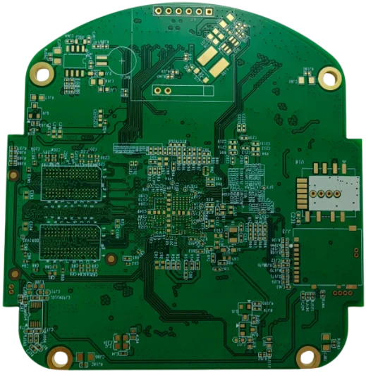
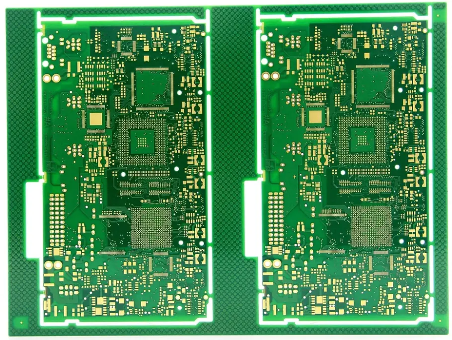
An Automotive Ethernet PCB prototype represents the physical realization of high-speed vehicle networking designs intended for testing and validation. Unlike traditional CAN or LIN buses, which operate at lower speeds, Automotive Ethernet brings high-bandwidth data transmission (from 100 Mbps to 10 Gbps) into the harsh environment of a vehicle.
The primary distinction between a standard Ethernet PCB and an automotive version lies in the physical layer (PHY). Automotive Ethernet typically uses a single unshielded twisted pair (UTP) for full-duplex communication to reduce cable weight and cost. This places an immense burden on the PCB design to reject noise and maintain signal integrity.
When you develop an Automotive Ethernet PCB prototype, you are not just routing traces; you are engineering a transmission line system that must survive vibration, thermal shock, and electromagnetic interference. At APTPCB (APTPCB PCB Factory), we see that successful prototypes bridge the gap between theoretical simulation and mass production reality. They prove that the chosen stackup, materials, and layout can handle the rigorous demands of modern vehicle architectures, such as ADAS (Advanced Driver Assistance Systems) and zonal controllers.
Metrics that matter (how to evaluate quality)
Building on the definition of high-speed performance, we must quantify what "good" looks like. You cannot improve what you cannot measure. When evaluating an Automotive Ethernet PCB prototype, specific signal integrity metrics determine pass or fail.
The following table outlines the critical metrics that designers and manufacturers must monitor.
| Metric | Why it matters | Typical range or influencing factors | How to measure |
|---|---|---|---|
| Differential Impedance | Mismatches cause signal reflections, reducing data integrity. | 100 Ohms ±10% (or tighter ±5% for high speeds). Influenced by trace width, spacing, and dielectric height. | Time Domain Reflectometry (TDR) on test coupons or actual traces. |
| Insertion Loss | Measures how much signal power is lost as it travels down the trace. | -0.5 dB to -2.0 dB per inch depending on frequency. Influenced by copper roughness and dielectric loss tangent (Df). | Vector Network Analyzer (VNA) measuring S21 parameters. |
| Return Loss | Measures the amount of signal reflected back to the source. | < -20 dB is desirable. High return loss indicates poor impedance matching or connector discontinuities. | VNA measuring S11 parameters. |
| Mode Conversion | Indicates how much differential signal converts to common-mode noise (EMI). | < -40 dB. Critical for passing EMC compliance tests. Caused by asymmetry in the differential pair. | VNA measuring mixed-mode S-parameters (Scd21). |
| Propagation Delay Skew | The time difference between the positive and negative signals in a pair. | < 5 ps per inch. Caused by length mismatch or fiber weave effect. | TDR or high-bandwidth oscilloscope. |
| Glass Transition Temp (Tg) | Determines the PCB's ability to withstand thermal stress without delamination. | > 170°C for automotive applications (High-Tg FR4). | Thermal Mechanical Analysis (TMA) or DSC. |
| Dielectric Constant (Dk) | Affects signal propagation speed and impedance dimensions. | 3.0 - 4.5. Stable Dk over frequency and temperature is vital for automotive environments. | Resonator method or calculated from stackup tests. |
Using tools like an Impedance Calculator early in the design phase helps align these metrics with manufacturable stackups.
Selection guidance by scenario (trade-offs)
Once you understand the metrics, the next step is applying them to your specific use case. Not every Automotive Ethernet PCB prototype requires the most expensive materials. The "best" choice depends on the data rate, location in the vehicle, and cost constraints.
Here are six common scenarios and the recommended trade-offs for each.
1. ADAS Camera Module (High Speed, Small Form Factor)
- Requirement: 1 Gbps to 10 Gbps data link; extremely tight space constraints.
- Trade-off: You must prioritize signal integrity over cost.
- Recommendation: Use High-Performance materials (like Megtron 6 or similar) to minimize loss. Use HDI (High Density Interconnect) with blind/buried vias to save space.
- Risk: Standard FR4 will cause too much attenuation at high frequencies, leading to link drops.
2. Infotainment Head Unit (Moderate Speed, Complex Routing)
- Requirement: Multiple 1 Gbps links; complex processor fan-out.
- Trade-off: Layer count vs. board size.
- Recommendation: A 10-12 layer board using Mid-Loss FR4. Focus on solid ground planes to isolate analog audio from digital Ethernet signals.
- Risk: Inadequate layer count forces reference plane splits, destroying return paths and creating EMI issues.
3. Body Control Gateway (Lower Speed, Cost Sensitive)
- Requirement: 100BASE-T1 (100 Mbps); connects many low-speed CAN buses.
- Trade-off: Cost is the primary driver.
- Recommendation: Standard High-Tg FR4 is usually sufficient. Keep traces short.
- Risk: Over-specifying materials here wastes budget. However, ensure the connector footprints are robust against vibration.
4. Powertrain Control (Harsh Environment)
- Requirement: 100 Mbps; extreme heat and vibration.
- Trade-off: Thermal reliability over electrical speed.
- Recommendation: Heavy copper (2oz+) for current carrying and very High-Tg (>180°C) materials. Ceramic-filled laminates may be needed for thermal expansion matching.
- Risk: Standard epoxy resin may soften or delaminate in the engine bay environment.
5. Diagnostic Interface (DoIP)
- Requirement: Interface with external service tools; high ESD exposure.
- Trade-off: Protection vs. Signal Integrity.
- Recommendation: Place robust ESD protection diodes close to the connector. Use controlled impedance traces but allow for the capacitance of protection devices.
- Risk: Placing ESD protection too far from the connector allows high-voltage spikes to damage the PHY before they are clamped.
6. Zone Controller (Mixed Signal)
- Requirement: Aggregates sensors and actuators; mix of power and data.
- Trade-off: Power integrity vs. Signal integrity.
- Recommendation: Use thick power planes but keep Ethernet pairs on outer layers or strictly referenced inner layers away from switching regulators.
- Risk: Noisy power supplies coupling into the Ethernet pairs, causing packet loss.
From design to manufacturing (implementation checkpoints)

Selecting the right scenario sets the strategy, but execution determines success. Moving from a design file to a physical Automotive Ethernet PCB prototype requires a rigorous checklist.
Use these checkpoints to guide your Automotive Ethernet PCB design through manufacturing.
1. Stackup Verification
- Recommendation: Confirm the stackup with APTPCB before routing. Ensure the dielectric heights support 100-ohm differential impedance with manufacturable trace widths (e.g., 4-6 mils).
- Risk: Designing with theoretical values that do not match stocked materials leads to impedance mismatches.
- Acceptance: Manufacturer-approved stackup sheet.
2. Differential Pair Routing
- Recommendation: Route Ethernet pairs symmetrically. Keep them tightly coupled. Avoid 90-degree bends; use 45-degree miters or arcs.
- Risk: Asymmetry converts differential signals to common-mode noise (EMI).
- Acceptance: DRC (Design Rule Check) showing constant spacing and width.
3. Reference Plane Continuity
- Recommendation: Ensure every Ethernet pair has a solid, unbroken ground plane underneath it along the entire length.
- Risk: Crossing a split in the ground plane creates a large return current loop, acting as an antenna.
- Acceptance: Visual inspection of plane layers relative to signal layers.
4. Via Management
- Recommendation: Minimize layer transitions. If a via is necessary, place a ground stitching via (return via) within 50 mils of the signal via to maintain the return path.
- Risk: Vias create impedance discontinuities and stub resonance.
- Acceptance: Simulation of via transitions; use of backdrilling for speeds > 1 Gbps.
5. Length Matching (Skew Control)
- Recommendation: Match the lengths of the positive and negative lines within the pair to within 5 mils (0.127 mm).
- Risk: Skew causes mode conversion and closes the data eye diagram.
- Acceptance: CAD tool length reports.
6. Component Placement (MDI)
- Recommendation: Place the Common Mode Choke (CMC) and DC blocking capacitors as close to the connector as possible.
- Risk: Long traces between the connector and protection components increase noise susceptibility.
- Acceptance: Review placement against PHY manufacturer guidelines.
7. Fiber Weave Mitigation
- Recommendation: For 1000BASE-T1 and higher, route traces at a slight angle (e.g., 10 degrees) relative to the PCB fabric weave, or use "spread glass" materials.
- Risk: One leg of the pair travels over glass (Dk ~6) and the other over resin (Dk ~3), causing massive timing skew.
- Acceptance: Material datasheet verification or zigzag routing pattern.
8. Connector Footprint Accuracy
- Recommendation: Use automotive-grade connector footprints (e.g., H-MTD, MATEnet) with anti-pads on inner layers to reduce capacitance.
- Risk: Standard footprints often have too much parasitic capacitance for high-speed automotive links.
- Acceptance: 3D field solver simulation of the connector breakout region.
9. Surface Finish Selection
- Recommendation: Use ENIG (Electroless Nickel Immersion Gold) or Immersion Silver for flat pads and good conductivity.
- Risk: HASL (Hot Air Solder Leveling) is too uneven for fine-pitch components and high-frequency signals.
- Acceptance: Fabrication drawing note specifying finish.
10. DFM Review
- Recommendation: Run a comprehensive DFM Guideline check to ensure drill sizes, annular rings, and copper spacing meet production capabilities.
- Risk: Board house puts the job on hold due to impossible tolerances.
- Acceptance: Clean DFM report from the manufacturer.
Common mistakes (and the correct approach)
Even with a checklist, errors happen. In our experience with Automotive Ethernet PCB assembly, certain mistakes occur repeatedly. Avoiding these saves time and money.
Mistake: Treating Automotive Ethernet like CAN bus.
- Correction: CAN is robust and slow; Ethernet is sensitive and fast. You cannot T-tap or daisy-chain Ethernet traces. It must be point-to-point.
Mistake: Ignoring the "Stub" effect of vias.
- Correction: At high frequencies, the unused portion of a via (the stub) acts as a resonant antenna. Use blind vias or specify backdrilling to remove the stub.
Mistake: Routing over power planes instead of ground.
- Correction: Always reference high-speed signals to Ground (GND). Power planes are noisy and do not provide a stable return path.
Mistake: Placing crystals/oscillators near the Ethernet connector.
- Correction: Keep clock sources far away from I/O connectors to prevent clock harmonics from radiating out of the cable.
Mistake: Over-constraining the impedance tolerance.
- Correction: Asking for ±2% impedance is often impossible for standard manufacturing. ±10% is standard; ±5% is premium. Design the circuit to tolerate slight variations.
Mistake: Forgetting test points.
- Correction: You cannot probe a BGA ball. Include small, controlled-impedance test points or probe footprints if you need to debug the physical layer.
Mistake: Neglecting thermal management for the PHY.
- Correction: Gigabit PHYs run hot. Ensure there is a thermal pad and sufficient ground vias to transfer heat to the inner planes.
Mistake: Using the wrong connector for the cable type.
- Correction: Ensure the PCB connector matches the specific twisted pair (STP vs UTP) cabling requirements of the vehicle harness.
FAQ
Q: What is the difference between standard Ethernet and Automotive Ethernet? A: Standard Ethernet (like 100BASE-TX) uses two or four pairs of wires and magnetic isolation. Automotive Ethernet (like 100BASE-T1) uses a single twisted pair, is full-duplex, and is designed to be lighter and more resistant to automotive EMI.
Q: Can I use standard FR4 for an Automotive Ethernet PCB prototype? A: For 100BASE-T1 (100 Mbps), standard High-Tg FR4 is usually acceptable. For 1000BASE-T1 (1 Gbps) and higher, you should consider mid-loss or low-loss materials to maintain signal integrity over longer distances.
Q: Do I need to shield the PCB traces? A: Generally, no. Automotive Ethernet is designed to work on Unshielded Twisted Pair (UTP). However, you must use "Stripline" routing (traces sandwiched between two ground planes) for the best EMI performance, rather than "Microstrip" (traces on the surface).
Q: What is the maximum trace length for Automotive Ethernet on a PCB? A: There is no hard limit, but insertion loss is the constraint. Typically, keep traces under 10-15 cm (4-6 inches) if possible. If longer, you must calculate the total channel loss budget including the cable.
Q: How do I test the impedance of my prototype? A: You need to request an "Impedance Coupon" from your manufacturer or use a TDR (Time Domain Reflectometer) on the actual board traces.
Q: What is "Backdrilling" and do I need it? A: Backdrilling removes the unused portion of a plated through-hole (via stub). It is highly recommended for speeds of 1 Gbps and above to prevent signal reflection.
Q: Does APTPCB support automotive-grade materials? A: Yes, we stock a variety of automotive-grade laminates, including Rogers, Isola, and Panasonic Megtron series, suitable for high-reliability and high-frequency applications.
Q: What data do I need to send for a quote? A: Send Gerber files (RS-274X), a drill file, a stackup diagram (or request one), material specifications, and any special requirements like impedance control or backdrilling.
Related pages & tools
- Impedance Calculator – Verify your trace widths and spacing before design.
- DFM Guidelines – Ensure your design is manufacturable.
- Panasonic Megtron Materials – High-speed materials for Gigabit automotive applications.
Glossary (key terms)
| Term | Definition |
|---|---|
| 100BASE-T1 | Automotive Ethernet standard for 100 Mbps over a single unshielded twisted pair. |
| 1000BASE-T1 | Automotive Ethernet standard for 1 Gbps (Gigabit) over a single unshielded twisted pair. |
| MDI (Medium Dependent Interface) | The physical connector interface on the PCB connecting to the cabling. |
| PHY (Physical Layer Transceiver) | The chip that converts digital data into analog signals for transmission. |
| UTP (Unshielded Twisted Pair) | Cabling type used in automotive Ethernet; relies on twisting for noise rejection. |
| Differential Impedance | The impedance between two conductors in a differential pair, typically 100 Ohms. |
| Insertion Loss | The loss of signal power resulting from the insertion of a device or transmission line. |
| Return Loss | The ratio of reflected power to incident power, measuring impedance matching. |
| TDR (Time Domain Reflectometry) | A measurement technique used to determine the impedance profile of a trace. |
| Skew | The timing difference between the positive and negative signals of a differential pair. |
| CMC (Common Mode Choke) | A magnetic component used to filter out common-mode noise (EMI). |
| Backdrilling | A manufacturing process to remove the unused portion of a via (stub). |
| SQI (Signal Quality Indicator) | A metric provided by the PHY chip indicating the health of the received signal. |
| PAM3 | Pulse Amplitude Modulation 3-level; the encoding scheme used in 100BASE-T1. |
Conclusion (next steps)
Developing a robust Automotive Ethernet PCB prototype is a balancing act between electrical performance, mechanical reliability, and cost. It requires a shift in mindset from standard digital logic design to high-frequency transmission line engineering. By focusing on the metrics of impedance, loss, and skew, and by selecting the right materials for your specific vehicle scenario, you can ensure a successful validation phase.
Remember that the prototype is your proof of concept. It must be manufactured to the same rigorous standards as the final production unit to provide valid test data.
Ready to build your prototype? To get an accurate DFM review and quote from APTPCB, please prepare the following:
- Gerber Files: Including all copper layers, solder mask, and silkscreen.
- Stackup Request: Specify your desired layer count and total thickness.
- Impedance Requirements: Clearly mark which traces require 100-ohm control.
- Material Specs: Indicate if you need High-Tg FR4 or specialized high-speed laminates.
Contact us today to start your Automotive Ethernet PCB prototype journey with a partner who understands the road ahead.