Definition, scope, and who this guide is for
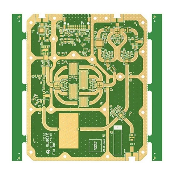
An automotive-grade On-board charger PCB (OBC PCB) is the critical power electronics backbone responsible for converting AC grid power into DC voltage to charge an electric vehicle’s high-voltage battery pack. Unlike standard industrial power boards, these PCBs must survive the harsh automotive environment—constant vibration, extreme thermal cycling, and high-voltage stress—while maintaining zero-failure reliability over a 15-year vehicle lifespan. They typically handle power ranges from 3.3kW to 22kW and voltages up to 800V, requiring specialized materials and heavy copper designs.
This guide is written for Hardware Engineers, PCB Procurement Leads, and Quality Managers who are tasked with sourcing or designing OBCs. It moves beyond basic datasheets to address the commercial and technical realities of manufacturing. You will find actionable specifications to include in your RFQ, a breakdown of manufacturing risks that cause field failures, and a validation checklist to audit your suppliers effectively.
At APTPCB (APTPCB PCB Factory), we understand that the decision to source an automotive-grade On-board charger PCB is not just about price per square inch; it is about mitigating liability and ensuring safety. This playbook consolidates best practices to help you navigate the complex trade-offs between thermal performance, electrical isolation, and manufacturability, ensuring your product scales from prototype to mass production without costly redesigns.
When to use this approach (and when not to)
Understanding when to deploy a fully specified automotive-grade On-board charger PCB versus a standard industrial power board is crucial for cost and reliability management.
Use an automotive-grade OBC PCB when:
- Voltage exceeds 400V: The board must handle high-voltage transients and requires strict Comparative Tracking Index (CTI) ratings to prevent arcing.
- Thermal density is high: You are using wide-bandgap semiconductors (SiC/GaN) that generate significant localized heat, requiring heavy copper or metal-core technologies.
- Vibration is constant: The unit is mounted directly to the vehicle chassis or powertrain, subjecting solder joints to continuous mechanical stress.
- Liability is a factor: The application involves a passenger vehicle where failure could lead to fire or loss of control, necessitating IATF 16949 compliance and PPAP documentation.
- Lifespan is critical: The product must operate for 10-15 years without degradation, unlike consumer electronics which may only need to last 3-5 years.
Consider a standard industrial PCB approach when:
- Stationary application: The charger is an off-board, wall-mounted unit (EVSE) that does not experience vehicle vibration or road debris.
- Low voltage/power: The application is a low-power auxiliary charger (under 1kW) where standard FR4 and 1oz copper suffice.
- Prototype/Proof of Concept: You are in the early stages of validating a circuit topology on a benchtop and do not yet need automotive-grade reliability testing.
- Non-critical accessory: The board powers a non-essential cabin feature that does not impact vehicle safety or propulsion.
Specs to define (materials, isolation, stackup, tolerances)
Defining the correct specifications upfront prevents technical queries from stalling your project. Below are the recommended baseline specs for a robust automotive-grade On-board charger PCB.
- Base Material (Laminate): High-Tg FR4 (Tg > 170°C) is mandatory to withstand soldering temperatures and operating heat. For higher power density, consider ceramic-filled laminates for better thermal conductivity.
- Comparative Tracking Index (CTI): Specify PLC 0 or PLC 1 (CTI ≥ 600V). This is non-negotiable for 400V/800V systems to prevent electrical breakdown and carbon tracking between traces.
- Copper Weight: Inner layers typically require 2oz to 4oz; outer layers may go up to 6oz or more depending on current requirements. Heavy copper is essential for minimizing $I^2R$ losses.
- Dielectric Thickness: Ensure sufficient prepreg thickness (minimum 2-3 plies) between high-voltage layers to pass Hi-Pot testing (typically 2500V AC or higher).
- Surface Finish: Immersion Silver (ImAg) or ENIG (Electroless Nickel Immersion Gold) are preferred for flat pads (essential for planar transformers and large MOSFETs) and wire bonding capabilities. HASL is generally avoided due to unevenness.
- Solder Mask: Use high-temperature, automotive-qualified solder mask (often green or black) that resists cracking under thermal cycling. Minimum dam width should be 4mil to prevent solder bridging on fine-pitch components.
- Via Structure: Plugged and capped vias (VIPPO) in thermal pads are often required to conduct heat away from power components without wicking solder away from the joint.
- Dimensional Stability: Tight tolerances (±10% or better) on overall thickness are critical if the PCB interfaces with a cold plate or heatsink via a thermal interface material (TIM).
- Cleanliness: Specify ionic contamination levels below 1.56 µg/cm² NaCl equivalent to prevent electrochemical migration (dendrite growth) in humid environments.
- Traceability: Laser marking of QR codes or Data Matrix codes on the PCB waste strip or the board itself for lot tracking down to the panel level.
- IPC Class: Specify IPC-6012 Class 3 for high reliability. This ensures stricter criteria for plating thickness, annular rings, and visual defects compared to standard consumer electronics (Class 2).
- Thermal Management: If using an automotive-grade SiC rectifier board sub-assembly, specify the thermal conductivity of the dielectric layer (e.g., 2.0 W/m·K or higher) to ensure rapid heat transfer to the heatsink.
Manufacturing risks (root causes & prevention)
High-voltage and high-current designs introduce specific failure modes. Understanding these risks helps you audit your supplier's process controls.
- Conductive Anodic Filament (CAF) Growth:
- Root Cause: Electrochemical migration along the glass fibers inside the PCB laminate, triggered by high voltage bias and humidity.
- Detection: CAF testing (1000 hours at 85°C/85% RH with bias).
- Prevention: Use "CAF-resistant" materials and ensure proper drill hit accuracy to avoid fracturing glass bundles.
- Heavy Copper Etch Factor Issues:
- Root Cause: Etching thick copper (e.g., 4oz) takes longer, leading to trapezoidal trace profiles (undercut) which reduces the effective cross-sectional area.
- Detection: Microsection analysis (cross-sectioning).
- Prevention: Suppliers must apply etch compensation factors to artwork and use multiple etch cycles for very heavy copper.
- Thermal Stress Delamination:
- Root Cause: Mismatch in CTE (Coefficient of Thermal Expansion) between copper, resin, and glass during reflow or operation.
- Detection: TMA (Thermomechanical Analysis) and thermal shock testing.
- Prevention: Use high-Tg, low-CTE materials and balance copper distribution on all layers to prevent warping.
- Solder Joint Fatigue:
- Root Cause: Vibration and thermal cycling cause solder joints to crack, especially on heavy components like inductors or transformers.
- Detection: Vibration testing and shear testing.
- Prevention: Use underfill for large BGAs/QFNs and ensure robust pad designs. For heavy through-hole parts, ensure 100% barrel fill.
- Plated Through Hole (PTH) Cracking:
- Root Cause: Z-axis expansion of the PCB stresses the copper barrel plating.
- Detection: Interconnect Stress Test (IST).
- Prevention: Ensure minimum copper plating thickness in holes averages 25µm (Class 3 requirement) and use resin systems with lower Z-axis expansion.
- Resin Recession:
- Root Cause: Resin shrinking away from the copper barrel during thermal excursions.
- Detection: Microsectioning after thermal stress.
- Prevention: Proper lamination cycle parameters (pressure/temp/vacuum) to ensure full cure.
- Foreign Object Debris (FOD):
- Root Cause: Conductive dust or debris left on the board before solder mask application.
- Detection: AOI (Automated Optical Inspection) and electrical testing.
- Prevention: Cleanroom manufacturing environment and aggressive cleaning processes before coating.
- Impedance Mismatch in Control Lines:
- Root Cause: Variation in dielectric thickness or trace width affecting CAN/LIN bus signals.
- Detection: TDR (Time Domain Reflectometry) testing on coupons.
- Prevention: Strict control of stackup and etching processes.
- Warp and Twist:
- Root Cause: Unbalanced copper stackup (e.g., signal layer vs. power plane) causing bowing during reflow.
- Detection: Bow and twist measurement gauge.
- Prevention: Design with copper balance in mind; use "thieving" (copper pouring) in empty areas.
- Solder Mask Voiding/Peeling:
- Root Cause: Poor adhesion on copper surfaces or trapped volatiles.
- Detection: Tape test (adhesion test).
- Prevention: Proper surface preparation (scrubbing/chemical clean) before mask application.
Validation & acceptance (tests and pass criteria)

Validation ensures the automotive-grade On-board charger PCB meets the design intent before mass production.
- Electrical Continuity & Isolation (BBT):
- Objective: Verify no opens or shorts.
- Method: Flying probe or bed-of-nails tester.
- Criteria: 100% pass. Isolation resistance > 100MΩ at specified voltage.
- Hi-Pot Testing (Dielectric Withstand):
- Objective: Verify insulation between high-voltage primary and low-voltage secondary sides.
- Method: Apply high voltage (e.g., 2500V DC) for 60 seconds.
- Criteria: Leakage current < 1mA (or as specified); no breakdown.
- Microsection Analysis:
- Objective: Verify internal structure quality.
- Method: Cross-section a coupon from the production panel.
- Criteria: Copper thickness meets spec (e.g., >25µm in holes), no cracks, good registration.
- Solderability Test:
- Objective: Ensure pads will accept solder during assembly.
- Method: Dip and look or wetting balance test (J-STD-003).
- Criteria: >95% coverage of the pad with a smooth solder coating.
- Thermal Shock Test:
- Objective: Simulate rapid temperature changes.
- Method: -40°C to +125°C (or +150°C), 500 to 1000 cycles.
- Criteria: Change in resistance < 10%; no delamination or cracking.
- Ionic Contamination Test (ROSE):
- Objective: Ensure board cleanliness.
- Method: Resistivity of Solvent Extract.
- Criteria: < 1.56 µg/cm² NaCl equivalent.
- Impedance Control Verification:
- Objective: Verify signal integrity for comms lines.
- Method: TDR measurement on test coupons.
- Criteria: Measured impedance within ±10% of target (e.g., 90Ω or 100Ω).
- Peel Strength Test:
- Objective: Verify copper adhesion to laminate.
- Method: Pull copper strip at 90 degrees.
- Criteria: > 1.05 N/mm (or per IPC spec for the material).
- Glass Transition Temperature (Tg) Verification:
- Objective: Confirm material properties.
- Method: DSC (Differential Scanning Calorimetry).
- Criteria: Tg must meet or exceed the specified value (e.g., ≥ 170°C).
- Dimensional Verification:
- Objective: Ensure mechanical fit.
- Method: CMM (Coordinate Measuring Machine) or calipers.
- Criteria: All dimensions within drawing tolerances.
Supplier qualification checklist (RFQ, audit, traceability)
Use this checklist to vet potential partners. A supplier unable to provide these items is a risk to your supply chain.
Group 1: RFQ Inputs (What you must provide)
- Complete Gerber files (RS-274X or X2) with clear layer definitions.
- Fabrication drawing specifying IPC Class 3 requirements.
- Material specifications (Tg, CTI, Halogen-free status).
- Stackup diagram with impedance requirements and copper weights.
- Drill chart distinguishing plated vs. non-plated holes.
- Panelization requirements (array drawing) for assembly efficiency.
- Special process notes (e.g., edge plating, countersink, filled vias).
- Volume projections (EAU) and batch sizes for pricing tiers.
- Packaging requirements (vacuum pack, desiccant, humidity indicator card).
Group 2: Capability Proof (What they must show)
- IATF 16949 certification (current and valid).
- UL file number for the specific stackup/material combination.
- Equipment list showing capability for heavy copper etching and heavy-duty lamination.
- In-house lab capabilities (Microsection, TDR, X-Ray fluorescence for finish thickness).
- DFM report examples showing they can catch issues before fab.
- Experience with similar high-reliability boards (e.g., automotive-grade BMS balancing board or automotive-grade SiC rectifier board).
- Capacity analysis demonstrating ability to handle your ramp-up.
Group 3: Quality System & Traceability
- PPAP (Production Part Approval Process) Level 3 capability.
- PFMEA (Process Failure Mode and Effects Analysis) availability for review.
- Control Plan detailing inspection points for every process step.
- Traceability system that links a specific PCB ID to raw material lots (copper, prepreg).
- MSA (Measurement System Analysis) for key inspection equipment.
- SPC (Statistical Process Control) charts for critical parameters (plating thickness, etch width).
Group 4: Change Control & Delivery
- PCN (Process Change Notification) policy—guaranteeing no changes without approval.
- Buffer stock agreement options for fluctuating demand.
- Disaster recovery plan (risk management).
- RMA process and turnaround time for failure analysis (8D reports).
- Logistics partners and Incoterms flexibility.
Decision guidance (trade-offs and decision rules)
Engineering is the art of compromise. Here is how to navigate common trade-offs in OBC PCB design.
- Heavy Copper vs. Embedded Busbar:
- Trade-off: Heavy copper (4oz+) is expensive and limits fine-line capability. Embedded busbars carry massive current but increase stackup complexity.
- Decision Rule: If current is < 100A, stick to heavy copper traces. If > 100A, consider embedded busbars or mechanical busbars to save PCB cost.
- FR4 vs. Metal Core (IMS):
- Trade-off: FR4 allows multilayer routing but has poor thermal conductivity. IMS is excellent for heat but limited to 1-2 layers.
- Decision Rule: Use FR4 for the main control and logic board. Use IMS (or a hybrid stackup) specifically for the power stage if you cannot use discrete power modules.
- Integrated vs. Modular Design:
- Trade-off: A single large PCB reduces interconnects but increases replacement cost. Modular designs (separate control and power boards) are easier to service but add connector failure points.
- Decision Rule: For high-volume, optimized designs, go integrated. For high-power units (>11kW) where power stages might vary, keep the automotive-grade SiC rectifier board modular.
- HDI vs. Standard Through-Hole:
- Trade-off: HDI (High Density Interconnect) saves space but costs more.
- Decision Rule: Avoid HDI for the high-power section. Only use HDI if the digital control section (MCU/FPGA) is extremely dense and space-constrained.
- Signal Integrity vs. Power Integrity:
- Trade-off: Large power planes are good for power but can couple noise into sensitive signals.
- Decision Rule: Physically separate the high-voltage power section from the low-voltage control section. Use a split ground plane with a bridge or opto-isolators. This is similar to the isolation required in an automotive-grade ECG acquisition board, where patient safety (isolation) is paramount, just as vehicle safety is here.
FAQ (cost, lead time, Design for Manufacturability (DFM) files, testing)
Q: What is the typical cost driver for an automotive-grade On-board charger PCB? A: The primary cost drivers are the heavy copper weight (commodity cost), the high-performance laminate material (High-Tg/High-CTI), and the rigorous testing requirements (Class 3 inspection, PPAP). Expect a 30-50% premium over standard industrial boards.
Q: How does the lead time for automotive-grade On-board charger PCB compare to standard PCBs? A: Standard prototypes might take 5-7 days, but automotive prototypes often take 10-15 days due to additional testing and material availability. Mass production lead times are typically 4-6 weeks, plus transit.
Q: What specific DFM files are needed for an accurate quote? A: Beyond Gerbers, you must supply a detailed stackup drawing, material datasheet requirements (or IPC equivalent), and a drill drawing that clearly identifies hole tolerances. For automotive-grade 48V VRM board sections integrated into the OBC, ensure thermal via patterns are clearly defined.
Q: Can we use standard FR4 for an automotive-grade On-board charger PCB? A: Generally, no. Standard FR4 often lacks the CTI rating (>600V) and thermal robustness (Tg > 170°C) required for OBC applications. You must specify automotive-grade laminates designed for high-voltage and high-temperature endurance.
Q: What are the acceptance criteria for automotive-grade On-board charger PCB testing? A: Acceptance is based on IPC-6012 Class 3. This means no breakout of holes, stricter annular ring requirements, and zero tolerance for cracks or delamination after thermal stress.
Q: How do you handle the high-frequency noise from the switching regulators? A: We recommend specific stackups with shielding layers. Similar to an automotive-grade Beamforming module board, proper grounding and shielding are essential to pass EMC requirements (CISPR 25).
Q: Do you support the manufacturing of the BMS section if it's integrated? A: Yes, we manufacture integrated designs that include the automotive-grade BMS balancing board functionality, provided the layout maintains sufficient isolation distances (creepage and clearance) between the high-voltage charging path and the battery monitoring circuits.
Q: What surface finish is best for wire bonding on the power stage? A: ENEPIG (Electroless Nickel Electroless Palladium Immersion Gold) or thick soft gold is preferred for wire bonding. However, for most standard OBCs using soldered components, Immersion Silver or ENIG is the standard choice for flatness and reliability.
Related pages & tools
- Automotive Electronics PCB Solutions – Explore our full range of automotive capabilities, from infotainment to powertrain.
- Heavy Copper PCB Manufacturing – Learn how we handle copper weights up to 10oz for high-current applications like OBCs.
- High Thermal PCB Technologies – Details on metal core and coin-insertion technologies for managing heat in power electronics.
- PCB Testing and Quality Assurance – A deep dive into our validation processes, including flying probe and functional testing.
- DFM Guidelines for Manufacturing – Download our design rules to ensure your OBC layout is optimized for production yield.
Request a quote (Design for Manufacturability (DFM) review + pricing)
Ready to validate your design? Contact our engineering team for a comprehensive DFM review and a detailed quotation.
To get the most accurate quote, please include:
- Gerber Files: RS-274X or ODB++ format.
- Fabrication Drawing: Specifying IPC Class 3, material Tg, and CTI requirements.
- Stackup Details: Copper weights per layer and dielectric thickness.
- Volume: Prototype quantity vs. estimated annual usage (EAU).
- Testing Requirements: Specific validation tests (e.g., CAF, Thermal Shock) required for PPAP.
Conclusion (next steps)
Sourcing an automotive-grade On-board charger PCB is a strategic decision that impacts the safety, efficiency, and longevity of an electric vehicle. By defining strict specifications for materials and tolerances, understanding the inherent manufacturing risks, and enforcing a rigorous validation plan, you can secure a reliable component that meets the demands of the modern automotive market. APTPCB is equipped to support this journey, offering the technical expertise and certified quality systems necessary to deliver high-performance power electronics at scale.